Useful defect contrast
Define the wafer stack, defect class and reference response.
Inspect, measure and process · Industry, inspection & flow
Connect defect contrast to the source, detector and scan recipe.
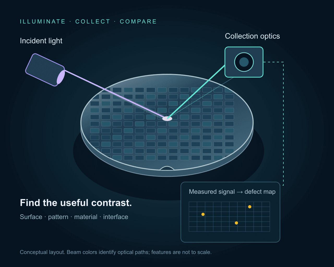
Define the wafer stack, defect class and reference response.
Choose geometry, polarization, filters and detector together.
Control illumination, focus, position and exposure timing.
Why the source matters
The correct source is defined at the sample or process—not at the laser aperture. Wavelength and operating mode set the interaction; stability, delivery, timing, and control determine whether it stays useful in the complete system.
Application workflow
Three decisions turn the application into a practical source specification.
Record material, films, pattern, process stage and defect classes. Distinguish surface scatter, reflected pattern contrast, luminescence and a transmitting infrared path.
Compare candidate wavelengths and geometries on representative samples. Measure background, delivered power and dose, then qualify the collection optics and detector band.
Match motion, focus control, exposure and data capture. Establish repeatability, missed-defect and nuisance-call criteria before defining throughput and supply scope.
Selection guide
These are starting architectures. Precisometer qualifies the final wavelength, output, delivery, control, and integration package against your setup.
Compare CW UV or visible excitation with dark-field or bright-field collection. Pattern references, alignment and stray-light control influence the result.
Match excitation and detection bands to the wafer material and defect response. Specify short-pulse excitation only when the measurement needs its timing.
Evaluate SWIR transmission or reflection on the actual stack, with an infrared-sensitive detector. Substrate thickness, doping, films and metal coverage limit optical access.
Source architecture
Particles, scratches and surface anomalies on bare wafers or films.
Compare UV and visible excitation on the actual surface. Collection angle, polarization and film background matter alongside wavelength.
Pattern differences, missing material and visible process anomalies.
Choose illumination angle, spectrum, coherence and polarization for pattern contrast. Laser illumination is one option; broadband illumination can also be appropriate.
Material and epitaxial nonuniformity, including suitable SiC and other compound-semiconductor defects.
Match excitation to the material, polytype and defect response. Specify emission filters and detector sensitivity separately from laser wavelength.
Accessible buried structures, cracks or bonded-interface features in a transmitting silicon stack.
Evaluate a wavelength such as 1550 nm against the actual wafer transmission and camera response. Thickness, doping, coatings and metal layers can restrict the path.
These existing catalogue examples illustrate different excitation architectures. Their model sheets govern power, stability, pulse duration and repetition rate. Match delivered power and dose to the sample; the highest catalogue power is not an inspection requirement.
CW UV · 266 nm
Evaluate UV surface contrast or material-specific excitation; confirm UV optics and delivered dose.
CW UV · 320 nm
An excitation option when the sample response and collection filters favor this UV line.
CW UV · 355 nm
Compare continuous UV excitation for scanning or luminescence measurements on the actual material.
Picosecond UV · 266 nm
Consider when the measurement requires short-pulse excitation. Specify pulse energy, timing and sample dose together.
Picosecond UV · 355 nm
A pulsed UV alternative for a timing-dependent experiment; verify its operating point against the model sheet.
Visible / violet CW · 405 nm
Evaluate reflected or scattered-light contrast with a matching camera, illumination profile and power control.
Infrared CW · 1550 nm
A candidate for a transmitting silicon path, with an infrared-sensitive detector and verified optical transmission.
Pair the source with the detection band, collection optics, focus control and scan synchronization. Define cleanliness, wafer handling, defect references and acceptance criteria before committing to a system architecture. A laser wavelength or semiconductor process-node name does not establish detection sensitivity.
Ready to specify
Specify wafer material and layer stack, defect classes and references, measurement method, excitation and detection bands, delivered dose, scan timing, repeatability and acceptance criteria.
Before you specify
Explore the optical methods, scan planner, source examples and a dedicated through-silicon imaging guide.
Semiconductor inspectionCompare dark-field scatter, bright-field reflection, photoluminescence and through-silicon SWIR. Explore optical paths, calculate sampling and motion, and build a source and detector brief.
Open guide Semiconductor inspection
Design a through-silicon inspection setup for wafers and ICs: choose transmission, reflection, or emission imaging; then match wavelength, NA, sampling, and camera.
Open guide