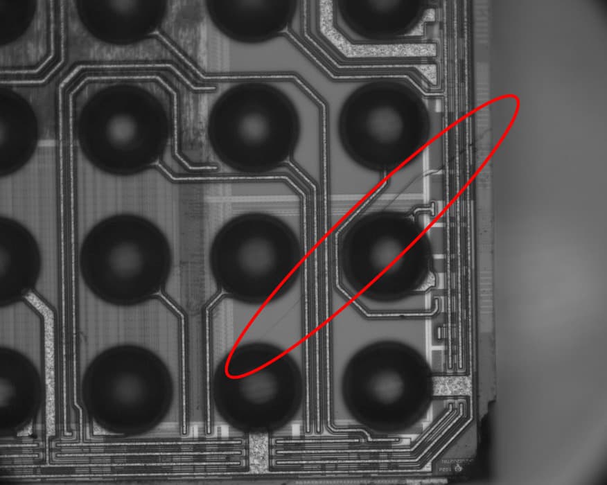
The short answer
The wafer is both the subject and the optical window.
Visible photons are absorbed strongly by bulk silicon, so a conventional microscope mostly reports the surface. Beyond the silicon band edge near 1100 nm, absorption falls and a useful fraction of SWIR light can pass through the substrate. An InGaAs camera on the other side records the light that survives.
Cracks, voids, interfaces, metal, doped regions, and changes in thickness alter that path. They appear as contrast without grinding, sectioning, or opening the device. The useful result is not “X-ray vision”; it is a fast, non-contact optical test with micrometre-scale resolution and familiar microscope mechanics.
E = hc / λ
At wavelengths longer than roughly 1100 nm, the photon energy drops below silicon's ~1.12 eV bandgap. That makes silicon a poor detector of SWIR—and a useful window for inspecting what sits behind it.
What it can reveal
Four semiconductor problems that suit SWIR.
The method is strongest when the defect changes transmission, reflection, or local emission—and when non-destructive access matters more than nanometre-scale detail.
Backside IC inspection
View die layout, bond structures, and gross process anomalies through an accessible silicon backside without removing the substrate.
Cracks, voids, and edge damage
Use transmission contrast to reveal cracks, inclusions, and interface defects that are difficult to distinguish in visible surface images.
Wafer and die alignment
Locate buried alignment marks for wafer-to-wafer or die-to-wafer processes when the optical path is not blocked by metal.
Photonics and emission work
Observe 1310 or 1550 nm sources, waveguide scatter, and other active near-infrared signals with suitable filters and exposure control.
1 · Choose the imaging geometry
Start from where the useful photons come from.
Camera selection comes later. First decide whether the measurement is transmission, reflection, or emission; each places different demands on access, illumination, and cooling.
Best starting point
Transmission
Place the SWIR source opposite the camera. Features become visible because cracks, interfaces, metals, and material changes attenuate or redirect the transmitted light.
- Strong through-silicon contrast
- Simple defect interpretation
- Good for wafers and loose die
Watch: Requires optical access to both sides and enough transmitted power through the actual stack.
Single-sided access
Reflection
Illuminate and collect from the same side. Reflection is practical for packaged parts or large wafers, and can reveal surface, near-surface, and interface contrast.
- One-sided access
- Easy mechanical integration
- Useful for alignment and surface context
Watch: Specular glare and weak subsurface contrast make coaxial illumination and flat-field correction important.
No illumination source
Emission
Image light generated by the powered device or photonic circuit. The setup prioritizes rejection of ambient light, sensor cooling, spectral filtering, and longer exposures.
- Telecom-band visibility
- Localizes active optical signals
- Works through transparent silicon paths
Watch: This is often photon-starved; use a cooled camera and do not assume a bright transmission setup will suit it.
2 · Select a wavelength
“Longer” is not automatically “better.”
Move far enough beyond the absorption edge to transmit through the sample, but no farther than the contrast requires. Longer wavelengths increase the diffraction limit, and the rest of the device stack can introduce its own absorption bands.
Good lab sequence
Test 1200 → 1300 → 1550 nm
Keep geometry, focus, exposure normalization, and flat-field correction fixed. Choose the wavelength that maximizes defect-to-background contrast—not the brightest raw frame.
| Band | Where it earns a test | Tradeoff to verify |
|---|---|---|
| 1050–1150 nm | Thin or lightly absorbing silicon; highest spatial resolution in this range | Near the silicon absorption edge, so transmission can change sharply with thickness, temperature, and material quality. |
| 1200–1350 nm | A practical first test for general through-silicon inspection and 1300 nm illumination | Usually a good resolution/transmission compromise; coatings and the full device stack still matter. |
| 1400–1550 nm | Thicker silicon paths, telecom photonics, and 1550 nm emission or illumination | Diffraction blur is larger, and water-rich adhesives or contamination can absorb strongly near 1450 nm. |
| 1550–1700 nm | Specialized long-wavelength contrast within standard InGaAs response | Check objective transmission, source power, sensor QE, and free-carrier absorption in doped silicon before committing. |
3 · Budget resolution honestly
Megapixels do not overrule diffraction.
SWIR inspection can resolve micrometre-scale features, but its wavelength is roughly three times longer than green light. The objective's numerical aperture therefore matters at least as much as the camera pixel pitch.
Use the camera to sample the optical image at least twice per resolved feature. Beyond that, extra pixels can still enlarge the field or improve registration, but they do not create finer optical detail.
Rayleigh resolution ≈ 0.61 λ / NA
Object-space pixel = camera pixel / magnification
Example at 1550 nm: a 10× / 0.26 NA objective resolves about 3.6 µm. A SWIR5000's 3.45 µm pixel becomes 0.345 µm at nominal 10×—comfortable oversampling. A 50× / 0.65 NA objective reaches about 1.45 µm before aberrations, focus, vibration, and sample contrast are considered.
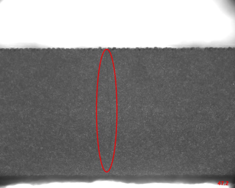
4 · Design the complete chain
The camera is one link in the measurement.
A good specification follows photons from source to decision. If one link is left undefined, the camera tends to become an expensive diagnostic for an illumination or optics problem.
SWIR illumination
Which wavelength and geometry create the contrast?
Start with a 1200, 1300, or 1550 nm LED. Add a diffuser or Köhler illumination for a uniform field, then test the real stack.
Sample and motion
Can both sides be reached, and must the field be tiled?
Plan for wafer diameter, package clearance, focus travel, XY repeatability, and whether automation needs a global shutter and hardware trigger.
SWIR objective
What NA, field, and working distance are practical?
Use SWIR-corrected objectives. NA sets diffraction resolution; working distance and field number decide whether the assembly physically fits.
InGaAs camera
Is the priority field, speed, or weak-signal performance?
Use small pixels and high megapixels for survey detail, larger pixels for sensitivity, and deeper TEC cooling for emission or long exposure.
Acquisition and QA
How will a defect become a repeatable measurement?
Lock exposure and gain, collect dark and flat fields, document focus, and validate thresholds on known-good and known-bad samples.
Specify this
- Smallest defect and required field of view
- Sample thickness, resistivity, finish, and access
- Transmission, reflection, or emission geometry
- Candidate wavelengths and available optical power
- Cycle time, trigger, interface, and automation needs
Do not specify only this
- “The highest resolution camera”
- Peak QE without the wavelength of interest
- Maximum frame rate without exposure and ROI
- A visible-light objective that happens to fit
- One attractive image without good/bad validation
Know the boundary
What SWIR microscopy does not replace.
Metal blocks the view
Dense metallization can hide features below it. SWIR needs a transmissive optical path.
It is not ambient thermal imaging
Room-temperature heat is measured in MWIR or LWIR, not by a standard 900–1700 nm camera.
Contrast is not chemical identity
A dark feature means attenuation or scattering changed; another method may be needed to identify the material.
It is not nanoscale metrology
At 1200–1550 nm, far-field diffraction keeps ordinary SWIR microscopy in the micrometre regime.
Precisometer SWIR options
Choose the camera after the measurement is clear.
These are the most relevant starting points for semiconductor microscopy and inspection. We can configure camera, interface, cooling, illumination, and microscope optics around your sample.
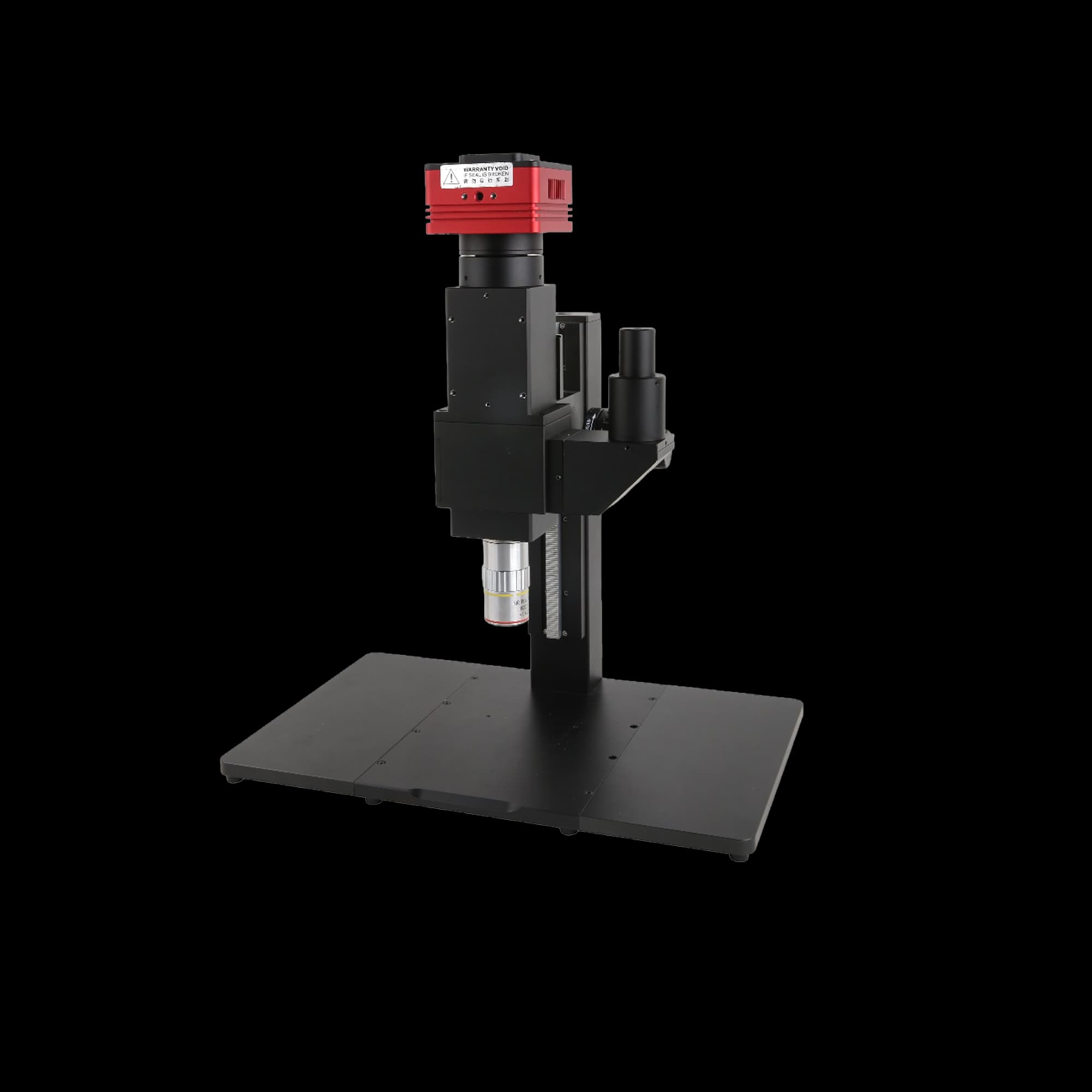
Complete microscopy route
BSM SWIR microscope systems
- 900–1700 nm optics
- 1200 / 1300 / 1400 / 1550 nm LEDs
- 5×–50× HR objectives
Choose this when you need the illumination, mechanics, tube optics, objectives, and C-mount camera interface to work as one inspection bench.
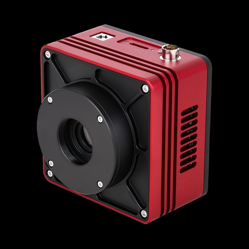
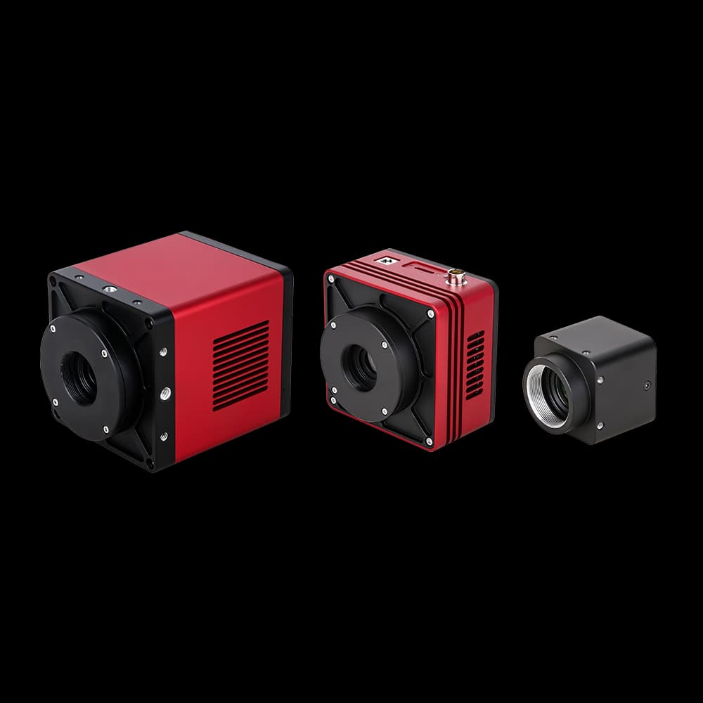
Resolution-first camera
SWIR5000 series
- 5.0 MP
- 3.45 µm pixels
- 400–1700 nm
- Up to 165 fps at 10GigE
The first camera to evaluate for high-detail wafer and die inspection. Its 5 MP sensor preserves a large field while the microscope optics set the true resolving power.
Speed and sensitivity balance
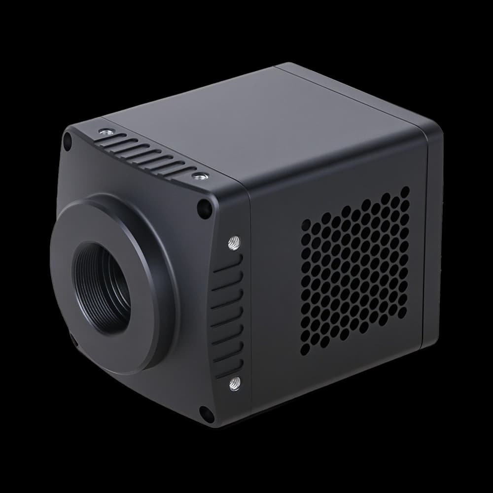
SWIR1300 series
- 1.3 MP
- 5 µm pixels
- 400–1700 nm
- 200 fps at USB3
A strong general-purpose choice for alignment, process observation, and inspection where full-resolution speed matters more than maximum pixel count.
Weak-signal specialist
SWIR1302 series
- 1.3 MP
- 15 µm pixels
- 900–1700 nm
- Deep TEC: 40 °C below ambient
The large-format, deep-cooled option for dim emission, long exposures, and photonic-device characterization where dark current matters more than compactness.
Common questions
The details that decide whether it works.
Why can SWIR microscopy see through silicon?
Crystalline silicon has a room-temperature bandgap near 1.12 eV. Photons longer than roughly 1100 nm carry too little energy for strong interband absorption, so bulk silicon becomes substantially more transmissive. Interfaces, cracks, metals, dopants, coatings, and other materials still change or block that light, creating image contrast.
What is the best wavelength for through-silicon inspection?
There is no universal best wavelength. A 1200 or 1300 nm LED is a sensible first test because it balances transmission and diffraction-limited resolution. A thicker or more absorbing stack may benefit from 1550 nm, while heavily doped silicon and water-rich adhesives can behave differently. Test the real wafer or package before fixing the illumination design.
Do I need an InGaAs camera?
For reliable imaging above about 1100 nm, yes. Silicon cameras can sometimes detect a bright source close to 1050 or 1064 nm, but their response collapses at the band edge. InGaAs provides useful sensitivity through the standard 900–1700 nm SWIR inspection band.
Can SWIR see through metal interconnects?
No. Metal remains opaque, so SWIR only reveals structures where the optical path passes through transmissive silicon and other compatible materials. Dense metal layers can mask underlying features; X-ray, acoustic, thermal, or destructive cross-section methods may be needed for those regions.
Is a 5 MP camera always better for microscopy?
No. More pixels can increase field of view or preserve detail, but the optical resolution is set mainly by wavelength and numerical aperture. At 1550 nm, a 0.65 NA objective has a Rayleigh resolution around 1.45 µm. Camera pixels much smaller than half that value in object space oversample the optics rather than reveal smaller features.
Is SWIR inspection the same as thermal imaging?
No. A SWIR camera mainly records reflected, transmitted, or emitted light from about 900 to 1700 nm. Room-temperature thermal radiation is concentrated at much longer mid- and long-wave infrared wavelengths. Use MWIR or LWIR equipment for ordinary temperature mapping.
Technical basis and further reading
Sources behind the guide.
01
Through-silicon MEMS inspection with a near-infrared laser scanning setupPeer-reviewed discussion of silicon transmission, Fresnel loss, doping, and metal-layer limitations.
02
Near-infrared inspection of wafer micro-cracks through dicing tapeApplied Optics paper describing non-destructive, on-tape crack inspection at 1100 nm.
03
SWIR imaging for semiconductor inspectionIndustry examples covering through-silicon alignment and inspection geometries.
04
Precisometer SWIR camera and BSM microscope specificationsSensor formats, cooling, interfaces, illumination wavelengths, and compatible microscope objectives.