Laser application guide
Designing a Raman measurement
One photon in ten million comes back shifted. Every choice in the chain — line, objective, grating, slit, detector — is about protecting that photon and reading it precisely enough to answer the question you actually have.
Protect the line
Envelope width and wavelength stability land directly on every band you measure.
Resolution costs window
One grating cannot both resolve a tenth of a wavenumber and show you 3200 of them.
A map is points × dwell
Halving the step size quadruples the acquisition. Sampling finer than the spot buys nothing.
The measurement chain
Four stages, each with one job.
Excitation
Put a clean, narrow, stable line on the sample
- Specify:
- Linewidth, spectral purity, power stability, wavelength drift
- Fails as:
- A broad or drifting line convolves onto every band and silently recalibrates the axis
Microscope
Focus tightly and collect from a defined volume
- Specify:
- Objective NA, confocal pinhole, working distance, stage accuracy
- Fails as:
- Signal from outside the intended volume — substrate, embedding medium, neighbouring grains
Spectrograph
Spread the light far enough to resolve the bands you care about
- Specify:
- Focal length, grating, slit width, stray light
- Fails as:
- Resolution and spectral window trade against each other — one grating cannot win both
Detector
Count very few photons without adding noise
- Specify:
- QE across your Stokes range, dark current, cooling, pixel count
- Fails as:
- Silicon goes blind past ~1050 nm, which caps the usable shift range at 785 nm excitation
Choosing the line
Signal, fluorescence, and where silicon stops.
Three constraints pull in different directions, and no wavelength wins all three.
| Line | Signal | Fluorescence | Shift range | Spatial | Typical samples |
|---|---|---|---|---|---|
| 532 nm | Strongest — scattering scales as ν⁴ | Highest risk on organics and biological samples | Full range to 9000 cm⁻¹ on silicon | Best: ~360 nm spot at NA 0.9 | Inorganics, carbon materials, 2D materials, minerals, semiconductors |
| 638 nm | About half of 532 nm | Lower — often the pragmatic middle | To ~6000 cm⁻¹ | ~430 nm spot | Pigments, resonance work, moderately fluorescent samples |
| 785 nm | ~4× weaker than 532 nm | Lowest — usually the only option on biological tissue | Capped near 3200 cm⁻¹ by the silicon cutoff | ~530 nm spot | Biological samples, pharmaceuticals, polymers, forensics |
A system with two or three switchable lines answers this by not answering it: run 532 nm for signal, fall back to 785 nm when the sample fluoresces. The excitation-wavelength guide works the trade through with an interactive lab.
Interactive
What your settings actually resolve.
Grating, slit, objective and step size, on a 320 mm spectrograph with a 2000-pixel detector. Watch the bands broaden and merge, the window shrink, and the map time climb.
Acquisition lab
Resolution, window, and how long the map takes
reference bands at the current instrument response — shaded region is one detector frame
Resolution
2.3 cm⁻¹
detector-limited
One-frame window
1574 cm⁻¹
partial fingerprint
Lateral resolution
433 nm
0.61λ/NA at 50× / 0.75
Confocal depth
1.3 µm
axial response
Dispersion
1.74 nm/mm
1800 g/mm, 320 mm
Map points
1,681
41 × 41 grid
Map time
29 min
1.0 s per point
Sampling
Undersampled
1.0 µm step vs 0.43 µm spot
Modelled on a 320 mm Czerny–Turner with a 2000-pixel detector at an assumed 14 µm pitch, using first-order grating relations with cos β taken as 1 — pessimistic by roughly 10%, so a real instrument does slightly better than this. Resolution combines the slit and two-pixel limits in quadrature; the reference bands are schematic, with realistic intrinsic widths. Map time counts 50 ms of stage settling per point and no autofocus or overhead.
What the spectrum reads
Four observables, four different specifications.
Naming which one you are after settles most of the argument about what to buy.
Peak position
Composition, and stress or strain
Band shift under tension or compression — the basis of stress mapping on silicon wafers
Wants sub-cm⁻¹ resolution: shifts are often a few tenths of a wavenumber
Peak width
Crystal quality, defects, disorder
Broadening from dislocations and amorphous content — GaN and SiC substrate assessment
Instrument response must be well below the band width, or you measure your own slit
Peak intensity
Concentration and phase fraction
Relative band areas for mixtures, polymorph ratios, and layer counting in 2D materials
Needs stable excitation power far more than it needs resolution
Polarization response
Crystal symmetry and orientation
Band intensity vs analyser angle — orientation of CVD diamond and single crystals
Requires a defined, stable polarization state through the whole collection path
Mapping
A spectrum per pixel.
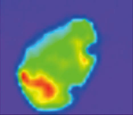
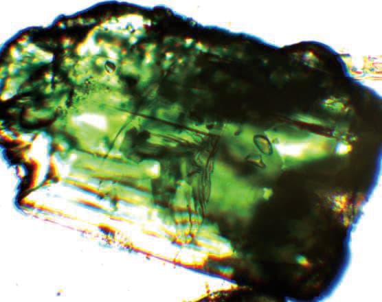
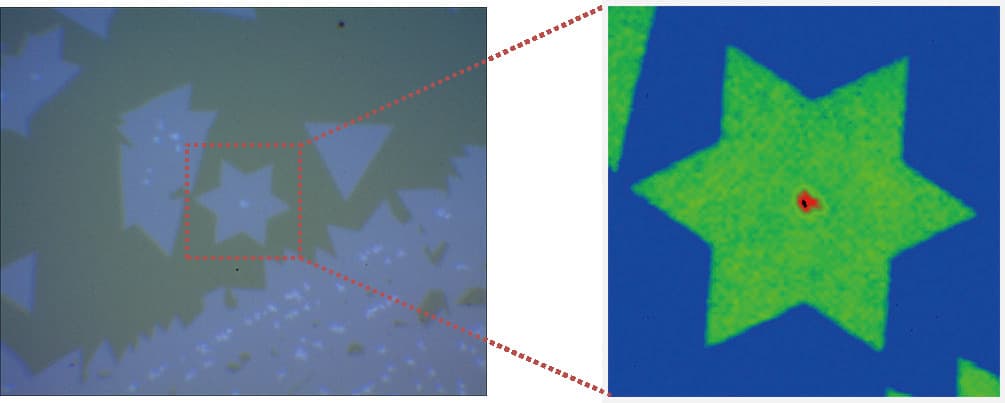
Raman mapping records a full spectrum at every point and builds an image from a chosen band — intensity, position, or width. Contrast comes from chemistry, not from stain or reflectivity, so features invisible in the optical image can dominate the Raman one.
The time budget
- points = (area/step)² — the term that hurts.
- 40 × 40 µm at 1 µm, 1 s/point ≈ 28 min.
- The same area at 0.5 µm ≈ 2.3 h.
- Stepping below ~0.4 µm at 532 nm oversamples the spot and buys nothing.
The turnkey answer
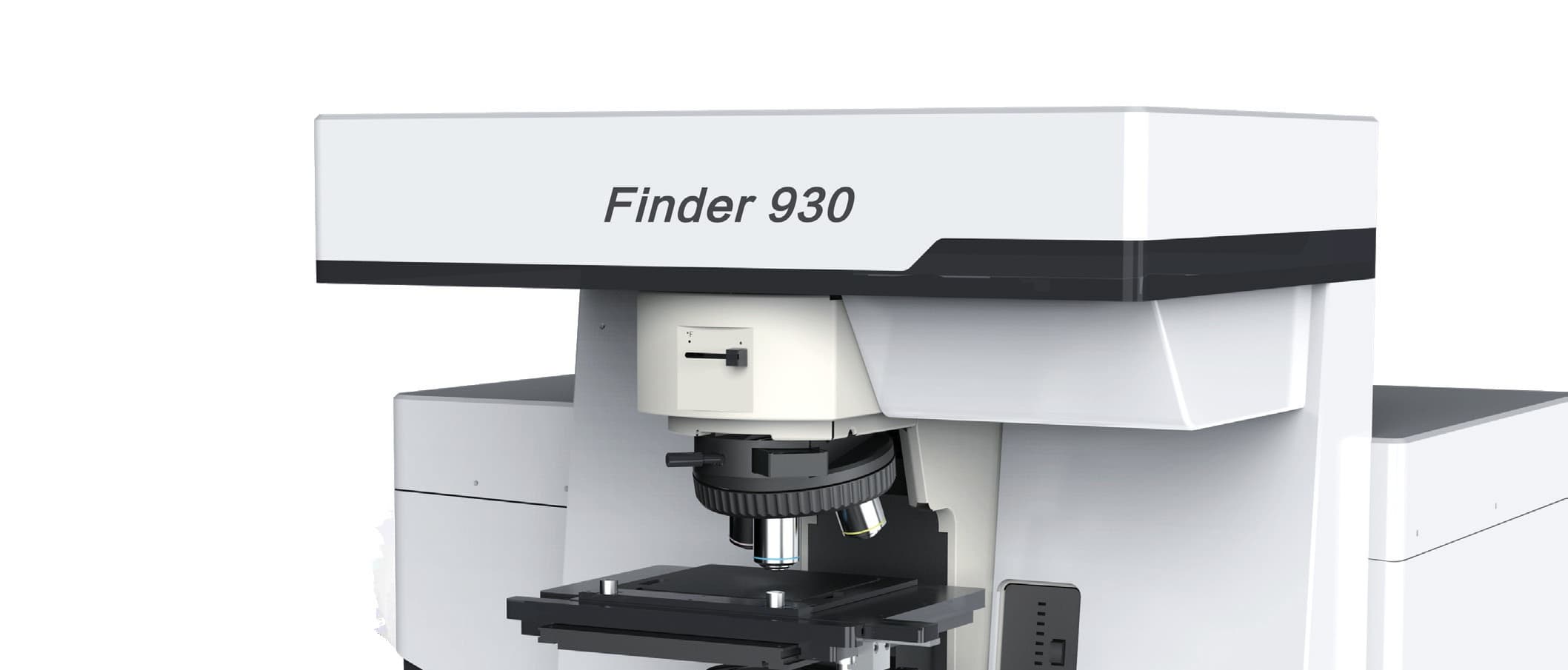
Finder 930 — the chain, integrated.
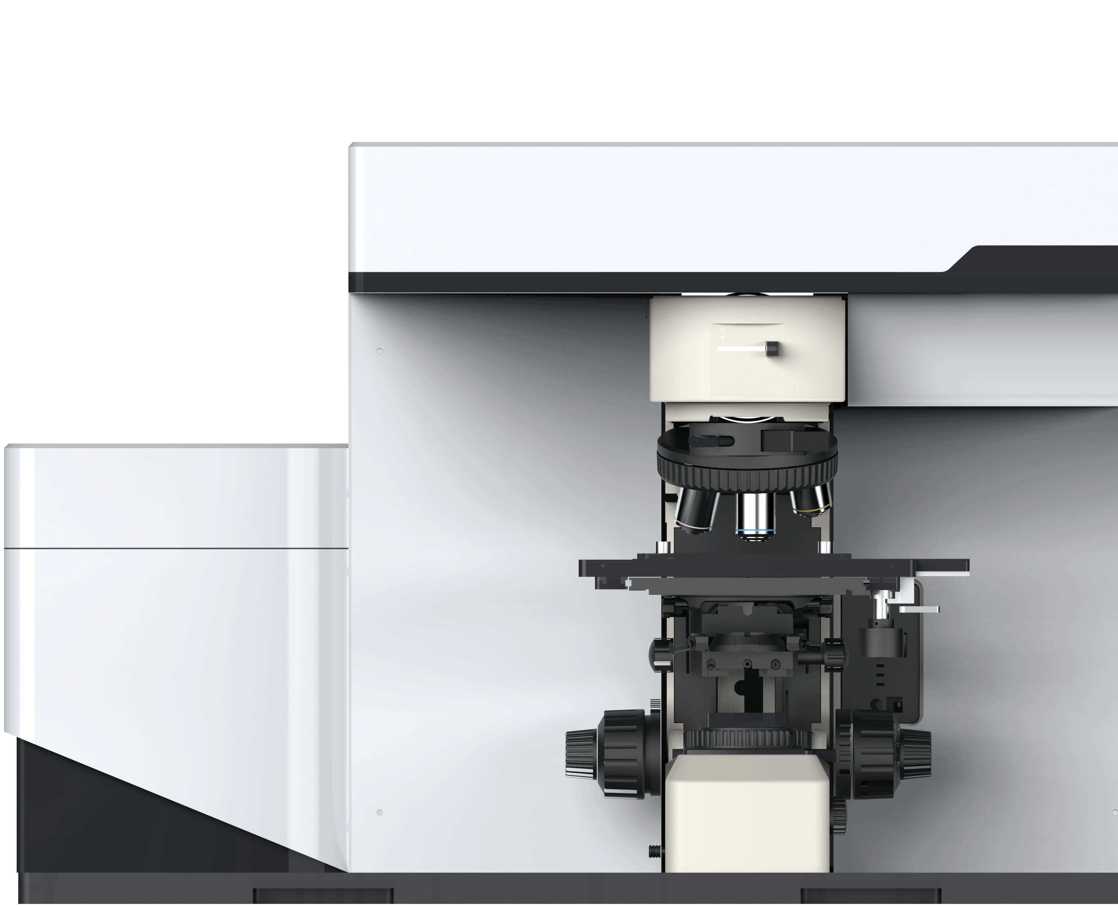
Every number in the lab above comes from this configuration: three switchable excitation lines, a 320 mm spectrograph with three gratings, a confocal microscope and a mapping stage, aligned as one instrument.
| Excitation | 532 nm standard; 638 and 785 nm optional, software-switchable |
|---|---|
| Spectrograph | 320 mm Czerny–Turner, F/4.2, stray light 1 × 10⁻⁵ |
| Gratings | 1800, 600 and 150 g/mm, blazed at 500 nm |
| Spectral resolution | < 1.5 cm⁻¹, typically 1.025 cm⁻¹ |
| Detector | 2000 × 256 CCD, QE > 90%, visible to NIR |
| Shift range | 80–9000 cm⁻¹ at 532 nm · 80–3200 cm⁻¹ at 785 nm |
| Lateral resolution | < 500 nm at 50 µm pinhole, 532 nm |
| Axial resolution | < 2 µm at 50 µm pinhole, 532 nm |
| Mapping stage | 75 × 50 mm travel, 1 µm accuracy, 50 nm minimum step |
| Objectives | 10×, 50× telephoto, 100×, semi-apochromatic |
In-situ accessories
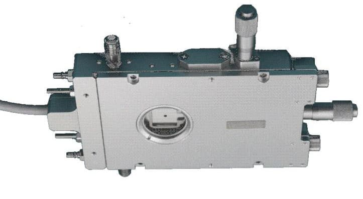
Cryostat
Bands narrow and separate at low temperature — often the only way to resolve close modes.
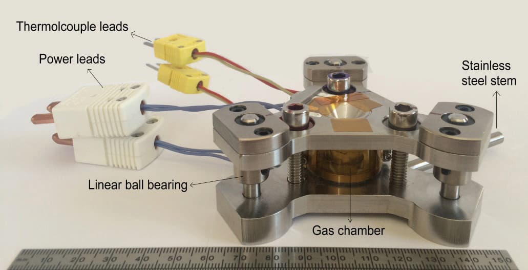
High-pressure cell
Diamond anvil work: phase transitions tracked through band shift under pressure.
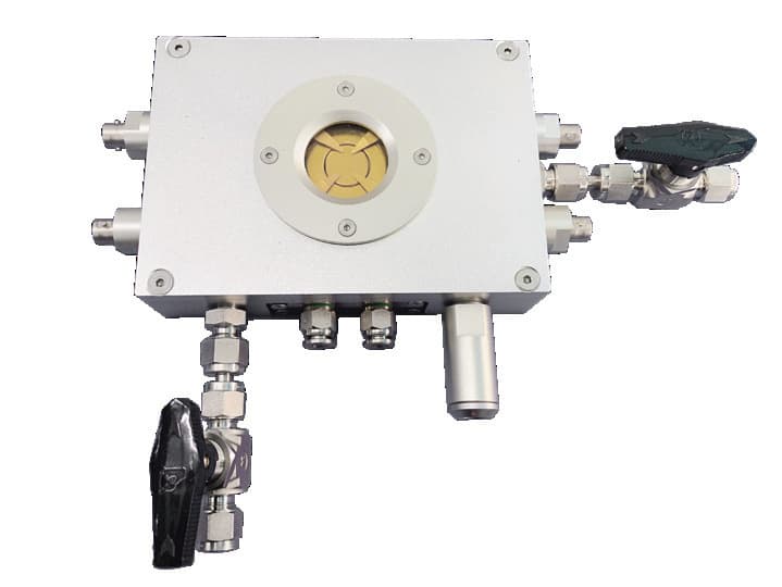
Electrochemical cell
In-situ battery and catalysis measurements while the cell is cycling.
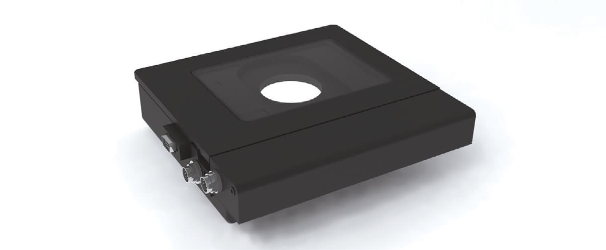
Motorized stage
75 × 50 mm of travel at 50 nm steps — the prerequisite for any map.
Excitation sources
When you build the path yourself.
For a component-built Raman setup, the line is the part worth over-specifying — it is the only element whose defects land on every band at once.
Lowest-noise 532 nm
FL-532-SLM
- 1~3000 mW
- <20 kHz
- <0.05% RIN(DC-3 MHz)
- <1.1
Single-frequency fibre laser: a narrow line adds effectively nothing to the measured band width, and low RIN keeps weak bands out of the noise.
Raman-configured 532 nm
MSL-U-532-Raman
- 1~500 mW
- <1 MHz
- <0.2%
- <1.1
A single-frequency DPSS built for Raman duty — narrow line and clean mode quality at modest power, without paying for fibre-laser coherence.
Wavelength-locked 785 nm
MLL-III-785-Lock
- 1~600 mW
- Low Noise Infrared Laser
- CW
- <0.2, <0.1, <0. 06
The fluorescence-avoidance workhorse. The lock matters more than the width: an unlocked diode drifts ~0.3 nm/°C, moving the whole shift axis between morning and afternoon.
Before you ask for a quote
Eight lines that make a quote comparable.
- Sample
- Material, expected bands, fluorescence behaviour, damage threshold, transparency.
- Excitation
- Wavelength, linewidth, power at the sample, stability over the acquisition.
- Shift range
- Lowest and highest wavenumber you must reach — decides grating and detector.
- Resolution
- The smallest shift or broadening you must resolve, in cm⁻¹, not nm.
- Optics
- Objective NA and working distance, confocal pinhole, sampling volume.
- Mapping
- Area, step size, dwell per point, and the total time you can afford.
- Environment
- Ambient, cryogenic, high pressure, electrochemical, or heated in situ.
- Filtering
- Edge or notch filters, and how close to the laser line you need to measure.
Questions
A few important nuances.
Which excitation wavelength should I use for Raman?
It is a three-way trade. Signal scales as ν⁴, so 532 nm gives roughly four times the scattering of 785 nm; but shorter wavelengths excite fluorescence that can bury the entire spectrum, and 785 nm is often the only option on biological or organic samples. The third constraint is silicon: at 785 nm the detector cutoff caps the usable shift near 3200 cm⁻¹, so the C–H region is reachable but little beyond it. Start from your sample’s fluorescence, then check the shift range you need.
How much spectral resolution do I actually need?
Match it to the observable. Identification from band positions is comfortable at 4–8 cm⁻¹. Stress and strain mapping reads shifts of a few tenths of a wavenumber and wants sub-cm⁻¹ resolution with a high-groove-density grating. Crystal-quality work measures band width, so the instrument response must be well below the intrinsic width or you are measuring your own slit function. Resolution is not free: it costs spectral window, and usually signal.
Why can I not have high resolution and a wide spectral window at once?
Both come from the same grating. A high groove density spreads the spectrum further, which resolves finer detail but pushes more of it off the edge of the detector. On a 320 mm spectrograph with a 2000-pixel sensor, 1800 g/mm resolves around 1 cm⁻¹ but shows roughly 1500 cm⁻¹ at a time, so fingerprint and C–H regions need two acquisitions. A 600 g/mm grating captures both in one frame at coarser resolution. The acquisition lab on this page makes the trade explicit.
What limits how fine a Raman map can be?
Two different things. The optics set the smallest meaningful step: the focused spot is about 0.61λ/NA, so around 360 nm at 532 nm with a 0.9 NA objective, and stepping much finer only oversamples the same volume. Time sets the practical limit: a map is points × dwell, and points scale as the square of the step. Halving the step quadruples the map. A 40 × 40 µm map at 1 µm steps and 1 s per point is about half an hour; at 0.5 µm steps it is over two hours.
Does the laser linewidth matter for Raman?
The width of the whole emission envelope matters; the single-mode linewidth almost never does. Every band is convolved with the laser’s emission profile, so a 0.3 nm diode adds roughly 1.6 cm⁻¹ of broadening at 785 nm while a single-frequency source adds effectively nothing. But 1 MHz and 1 kHz linewidths are equally invisible to any spectrograph. Pay for a narrow envelope and a stable centre wavelength; do not pay for coherence you cannot use.
Why does wavelength stability matter as much as linewidth?
Because the Raman axis is referenced to the laser line. A free-running diode moves about 0.3 nm per °C of case temperature, and at 785 nm every 0.1 nm of drift shifts the whole axis by roughly 1.6 cm⁻¹. That is larger than the shifts stress mapping is trying to measure, and it appears as a slow recalibration between morning and afternoon rather than as obvious noise. A volume Bragg grating pins the centre wavelength, which is why the locked variant is the standard 785 nm choice.
Going deeper
Related guides and instruments.
- Choosing a Raman excitation wavelength
The ν⁴ law, fluorescence background and detector cutoff, with an interactive wavelength lab.
- How to choose a spectrograph
Focal length, grating and slit as one decision, worked through real dispersion numbers.
- Laser specifications decoded
Linewidth vs spectral width, and which one your spectrometer can actually see.
- Finder 930
The confocal Raman platform these numbers come from — full specification and configuration.
- Raman spectroscopy at Precisometer
Instruments, components and measurement services across the Raman range.
- Spectrographs & monochromators
When the Raman path is built from components rather than bought as a platform.
Next step
Tell us the sample and the observable.
Material, the bands you need, the shift range, and whether you are after identity, stress, quality or a map. We will come back with the excitation line, grating and configuration that reach it — and say where a simpler setup is enough.