Back to Home
Knowledge Base & Application Note

Confocal RamanMicroscopy

How scattered laser light reveals what a material is made of — bond by bond, particle by particle. Walk through the physics, play with live spectra, and follow a worked application note on microplastic detection, with references throughout.

Stokes scatteringMolecular fingerprintsMicroplastic mapping3 live simulations

The idea in one paragraph

Light that carries a chemical signature

Shine a single-colour laser on almost any material and most light bounces off unchanged. But a vanishingly small fraction comes back shifted in colour, having traded energy with the molecule's vibrations. Measure those shifts and you measure the chemistry — no dyes, no contact, no sample destruction.

A confocal Raman microscope does this one diffraction-limited spot at a time. Add a motorized stage and the instrument turns a spectrum into a picture: a chemical map that shows not just what is present but exactly where.

< 500 nm
lateral resolution
532–785 nm
excitation lasers
80–4000 cm⁻¹
fingerprint range

The measurement chain

  1. 1
    Excite
    A monochromatic laser illuminates a sub-micron spot on the sample.
  2. 2
    Scatter
    A trace of photons scatter inelastically, shifted by molecular vibrations.
  3. 3
    Disperse
    A grating spreads the scattered light; a cooled CCD records the spectrum.
  4. 4
    Identify / map
    Peaks are matched to a library; a motorized stage builds a chemical image.

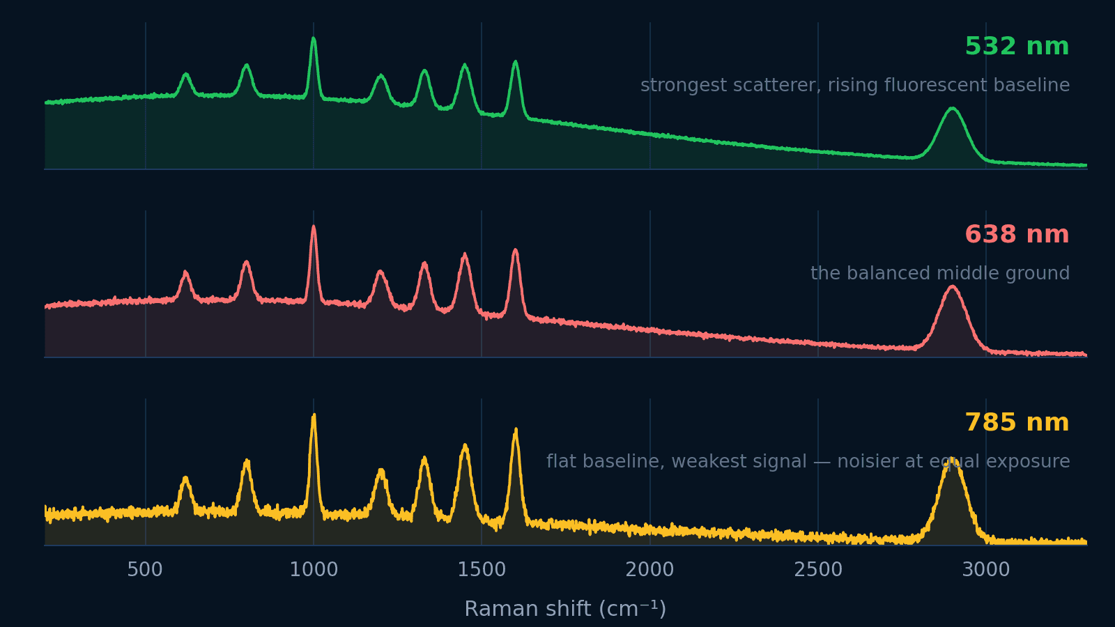
A redder excitation laser (638 or 785 nm) is often chosen to suppress fluorescence, which can otherwise swamp the weak Raman signal. [3]

The physics

Four ideas that make it work

From a single scattered photon to a full chemical map, the method rests on these four foundations.

Inelastic scattering[1]

When laser light hits a molecule, roughly one photon in a million scatters inelastically — exchanging a quantum of vibrational energy. That tiny colour shift is the Raman effect, discovered in 1928.

A molecular fingerprint[3]

Each chemical bond vibrates at a characteristic frequency, so the set of Raman shifts (in cm⁻¹) is unique to a compound and its structure — a label-free fingerprint that distinguishes PET from PE or diamond from graphite.

Confocal microscopy[8]

A pinhole rejects out-of-focus light so the signal comes from a sub-micron volume. Combined with a high-NA objective this gives < 500 nm lateral and ~2 µm depth resolution — spectroscopy on single particles.

Hyperspectral mapping[7]

Move the sample under the focus on a motorized stage and record a full spectrum at every pixel. The result is a chemical image: false-colour maps of composition, stress, crystallinity, or phase.

Δν̃ = 1/λ_laser − 1/λ_scattered
Raman shift in cm⁻¹ — independent of the laser used, set only by the molecule.
E_vib = h c Δν̃
Each shift equals a vibrational energy quantum of a specific bond.
I_antiStokes / I_Stokes ∝ e^(−hcΔν̃/kᴮT)
The Stokes/anti-Stokes ratio reports temperature.
Live simulation 1

Rayleigh, Stokes & anti-Stokes

Follow a photon as it is absorbed to a short-lived virtual state and re-emitted. Elastic Rayleigh scattering returns the same energy and carries no chemical information; the red-shifted Stokes line is the Raman signal we measure; the blue-shifted anti-Stokes line is weaker because it needs a pre-excited molecule.

Only about one in a million scattered photons is Raman-scattered. The tiny energy shift between the incoming and outgoing photon equals a molecular vibration — the quantity that becomes a chemical fingerprint.

Live simulation 2

Reading a molecular fingerprint

Switch between five common microplastics and several reference materials to see how each produces a distinct pattern of bands. PET's carbonyl at 1728 cm⁻¹, polystyrene's ring-breathing mode at 1001 cm⁻¹, PVC's C–Cl doublet near 640 cm⁻¹ — these are the diagnostic peaks an analyst looks for. Change the excitation laser to watch the fluorescence background rise and fall.

Microplastics
Other materials
Excitation laser
PET — polyethylene terephthalate

Grey shading is the fluorescence background. Switch to a redder laser and watch it collapse — the reason the Finder 930 offers 638 nm and 785 nm options for fluorescent samples.

Peak positions after standard polymer and materials Raman references; see Smith & Dent [3], Araujo et al. [6] and Ferrari et al. [10].

Where it is used

One instrument, many questions

Because the fingerprint is universal, the same confocal Raman platform serves environmental, industrial and life-science labs.

Environmental

Microplastic identification

Classify and count polymer particles down to ~1 µm on a filter and sort them by type (PET, PE, PP, PS, PVC).

Pharma / QC

Pharmaceutical polymorphs

Distinguish crystal forms of an active ingredient and detect counterfeits or contaminants non-destructively.

Electronics

Semiconductor stress[9]

The 520 cm⁻¹ silicon band shifts with strain — map mechanical stress across wafers and devices.

Nanomaterials

2D materials & carbon[10]

Count graphene layers from the 2D band and quantify defects from the D/G intensity ratio.

Geology

Minerals & gemstones

Identify mineral phases and inclusions, and authenticate gemstones from their vibrational spectra.

Life science

Cells & biomaterials

Probe protein, lipid and nucleic-acid content in cells and tissue without stains or labels.

Live simulation 3 · Featured application

Mapping microplastics on a filter

This is microplastic detection in miniature. Water is filtered so that suspended particles collect on a membrane; the Raman microscope then rasters across it, records a spectrum at each particle, and matches it to a polymer library. Press Run Raman map to scan, watch particles get classified and colour-coded, then click any particle to inspect the spectrum that identified it.

Raster the confocal spot across the filter; each particle is classified by its spectrum.

Particle inventory

0 particles
PET
0
PE
0
PP
0
PS
0
PVC
0

Workflow and classification approach after Käppler et al. [4], Lenz et al. [5], Araujo et al. [6] and Anger et al. [7].

Application note

Detecting microplastics in a water sample

A representative workflow for identifying and quantifying microplastic particles (~1–50 µm) in drinking, surface or waste water. Raman is the method of choice below ~20 µm, where it resolves smaller particles than FTIR and cleanly separates polymer types. Figures below are illustrative of the method, not a validated product specification.

Protocol

  1. 1. Filter a known volume (e.g. 1 L) onto a Raman-compatible membrane (silicon, gold-coated, or Al₂O₃).
  2. 2. If needed, digest organic matter (H₂O₂ / enzymatic) to reduce fluorescence and clutter.
  3. 3. Locate particles by optical/​dark-field imaging, then define a mapping region.
  4. 4. Acquire a Raman spectrum per particle; use 785 nm where fluorescence is high.
  5. 5. Match each spectrum against a polymer library; report type, size and count.

Diagnostic bands

PET1728, 1614, 1096 cm⁻¹
PE1440, 1296, 1063 cm⁻¹
PP1458, 809, 973 cm⁻¹
PS1001 (ring), 1602 cm⁻¹
PVC638 / 694 (C–Cl) cm⁻¹

Why Raman here

  • Resolves particles down to ~1 µm — below FTIR's practical limit.
  • Confidently separates polymer classes, including weathered fragments.
  • Also flags pigments and additives that hint at the particle's origin.
  • Non-destructive — particles stay intact for archiving or re-analysis.

Good-practice notes. Work in a clean, plastic-free environment and run procedural blanks — airborne fibres are a notorious source of false positives. Suppress fluorescence with a redder laser or mild oxidative digestion, keep laser power low to avoid burning dark or thin particles, and validate library matches with a correlation threshold. See Käppler et al. [4] and Araujo et al. [6].

Complementary technique

Where Raman meets microrheology

Raman tells you what a material is; optical-tweezers microrheology tells you how it flows and deforms. Together they give a complete picture of a soft or complex sample — chemistry and mechanics at the microscale.

Explore the microrheology knowledge note
Label-free chemical ID
Sub-micron chemical maps
Non-destructive analysis
Complements mechanical data
Companion guide

From the technique to the instrument

This note covers what Raman measures and what it can tell you. The design guide covers the other half — turning that into a specification: excitation wavelength, spectral resolution against the window you can capture at once, confocal sampling volume, and how long a map really takes.

Open the Raman measurement design guide
532 · 638 · 785 nm — signal against fluorescence
Grating and slit — resolution against spectral window
Interactive acquisition lab
Mapping: points × dwell, and what oversamples

References

  1. 1

    C. V. Raman, K. S. Krishnan, “A new type of secondary radiation,” Nature 121, 501–502 (1928).

    doi.org/10.1038/121501c0
  2. 2

    The Nobel Prize in Physics 1930 — Sir Chandrasekhara Venkata Raman, “for his work on the scattering of light and for the discovery of the effect named after him.” NobelPrize.org.

    www.nobelprize.org/prizes/physics/1930/summary/
  3. 3

    E. Smith, G. Dent, Modern Raman Spectroscopy: A Practical Approach, 2nd ed., Wiley (2019).

    doi.org/10.1002/9781119440598
  4. 4

    A. Käppler et al., “Analysis of environmental microplastics by vibrational microspectroscopy: FTIR, Raman or both?,” Analytical and Bioanalytical Chemistry 408, 8377–8391 (2016).

    doi.org/10.1007/s00216-016-9956-3
  5. 5

    R. Lenz et al., “A critical assessment of visual identification of marine microplastic using Raman spectroscopy for analysis improvement,” Marine Pollution Bulletin 100, 82–91 (2015).

    doi.org/10.1016/j.marpolbul.2015.09.026
  6. 6

    C. F. Araujo et al., “Identification of microplastics using Raman spectroscopy: Latest developments and future prospects,” Water Research 142, 426–440 (2018).

    doi.org/10.1016/j.watres.2018.05.060
  7. 7

    P. M. Anger et al., “Raman microspectroscopy as a tool for microplastic particle analysis,” TrAC Trends in Analytical Chemistry 109, 214–226 (2018).

    doi.org/10.1016/j.trac.2018.10.010
  8. 8

    N. J. Everall, “Confocal Raman microscopy: performance, pitfalls, and best practice,” Applied Spectroscopy 63(9), 245A–262A (2009).

    doi.org/10.1366/000370209789379196
  9. 9

    I. De Wolf, “Micro-Raman spectroscopy to study local mechanical stress in silicon integrated circuits,” Semiconductor Science and Technology 11, 139–154 (1996).

    doi.org/10.1088/0268-1242/11/2/001
  10. 10

    A. C. Ferrari et al., “Raman spectrum of graphene and graphene layers,” Physical Review Letters 97, 187401 (2006).

    doi.org/10.1103/PhysRevLett.97.187401

This note is educational. Simulated spectra use representative band positions and simplified line shapes; instrument performance figures are indicative and should be confirmed for your specific samples.

Put a chemical fingerprint on your samples

See how the Finder 930 confocal Raman platform can identify, map and quantify materials — from microplastics to semiconductors.

Before you specify

Guides for Raman system design

Excitation wavelength, the coherent alternative to spontaneous Raman, and the spectrograph that reads either of them out.
All guides