Back to Home
← All guides

Integrated photonics · 22 min

How to build a photonic integrated circuit test and alignment station

The die is usually fine. Getting light into it, holding the coupling peak, and resolving what comes back out is the hard part. Build the station around those three constraints and the bill of materials becomes surprisingly clear.

Edge vs gratingCoupling toleranceActive alignmentHigh-Q resonancesComplete test chain
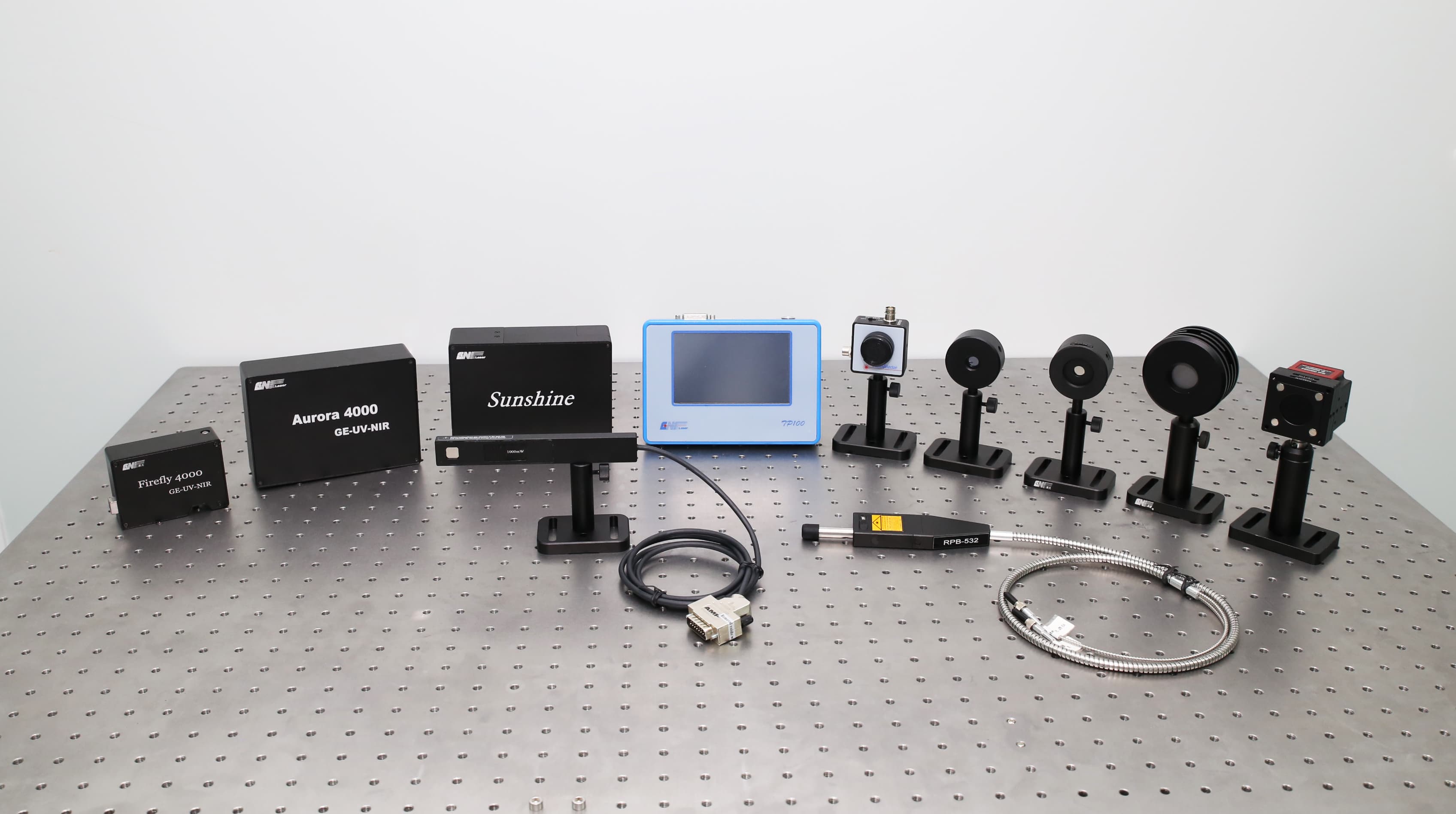
Optical measurement equipment suitable for a photonic integrated circuit test station
source → polarization → DUT → detector

Start with the interface

The station exists to solve one mode-matching problem.

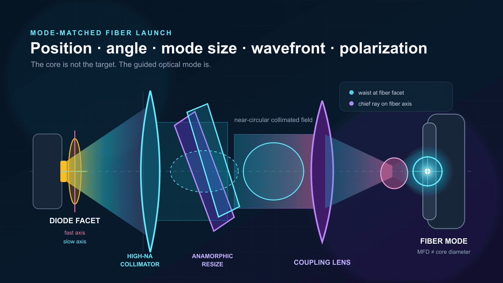
Standard telecom single-mode fibre carries a mode about 10.4 µm across. A bare silicon wire carries one well under 1 µm. Butt the two together naked and the mode mismatch alone costs about 20 dB. No six-axis stage can align power into a mode that does not spatially overlap in the first place.

That is why a useful PIC includes a spot-size converter or a grating coupler, why the station uses a lensed or high-NA fibre, and why the last micrometre of motion is split between coarse mechanics and a fine piezo. The source, polarization controller, VOA, switch, detector, and digitiser all exist to measure the resulting peak without distorting it.

The purchase order should therefore begin with platform, coupling scheme, mode size, device Q, and port count. Beginning with a stage catalogue produces a pile of axes; beginning with the optical interface produces a station.

Four coupled constraints

Fixing one exposes the next.

Mode mismatch

Standard telecom single-mode fibre has a mode-field diameter around 10.4 µm. A bare silicon waveguide mode is well under 1 µm. Put the two together without a spot-size converter and the mismatch term alone is about 20 dB — before offset, tilt, facet reflection, or roughness enters.

Sub-micron position

Once a lensed or ultra-high-NA fibre matches the expanded on-chip mode, the coupling peak becomes narrow. A manual stage can find the neighbourhood; it cannot reliably sit on the peak. The fine axis needs closed-loop motion and enough resolution to sample the peak rather than jump over it.

Polarization

PIC waveguides are strongly birefringent, and standard grating couplers are usually designed for TE. Ordinary single-mode fibre does not preserve a fixed state as it is moved or warmed. Polarization control is part of the measurement, not an accessory to add after the traces look wrong.

Temperature

A silicon resonance shifts by roughly 70 pm/K. At high Q, a small chuck-temperature change can move the line by a material fraction of its width during one sweep. A laser with excellent wavelength resolution still measures drift if the device is not held thermally still.

Choose the optical I/O

Edge coupling is an XYZ problem. Grating coupling is an angle problem.

The coupler is not a packaging detail. It changes the station mechanics, usable wavelength span, polarization workflow, and the point in manufacturing at which a die can be tested.

DecisionEdge couplerGrating coupler
Coupling lossLowest when a spot-size converter is matched to a lensed or UHNA fibre; facet quality and lateral offset add directly.Design-dependent and commonly higher than a good edge coupler; the penalty buys access from above.
Optical bandwidthBroad. A well-designed taper is not tied to a narrow phase-matching condition.Limited by the grating phase-matching band. Do not assume a coupler designed at one band stays efficient across the whole source sweep.
Polarization sensitivityStill platform-dependent, but both TE and TM structures can be reached with the right launch and waveguide design.Usually strongly selective; a standard one-dimensional silicon grating commonly accepts TE only.
Facet preparationNeeds an exposed, clean facet and usually dicing or polishing. The spot-size converter has to terminate where the fibre can reach it.No polished edge is required. The fibre approaches the top surface at the grating design angle.
Wafer-level testAwkward with ordinary fibres because the die edge is not exposed before dicing; specialist probes can do it, but complexity rises.The decisive advantage. Probe devices before dicing, reject weak dies early, and avoid spending packaging effort on known failures.
Hard alignment axisXYZ position. Small matched modes make the transverse peak narrow; longitudinal gap matters as the beam diffracts.Angle. Lateral capture is generous relative to edge coupling, but phase matching punishes theta error.

Grating couplers are a yield tool. Testing before dicing is not merely convenient optical access; it lets you reject weak dies before the expensive packaging steps begin.

Interactive

Turn mode sizes into stage requirements.

Compare five practical coupling schemes, add offset, tilt, and gap, then read the one-dB tolerances and the stage resolution implied by the optical peak. The calculation makes clear where a 2 µm manual stage stops being a fine stage.

Coupling and alignment lab

What your positioner actually has to achieve

Coupling scheme sets the mode sizes; the mode sizes set the tolerances; the tolerances set the stage. Work down that chain and the specification writes itself.

Coupling scheme

The workhorse of edge-coupled characterisation. Modes are nearly matched, so the loss is dominated by fabrication and Fresnel rather than overlap — at the cost of the tightest lateral tolerance on this list.

Mode radii

Fibre side1.4 µm
Chip side1.6 µm

300 nm

Transverse error in X or Y between the fibre core and the waveguide.

0.30°

Tilt between the fibre axis and the waveguide axis, or off the grating design angle.

5.0 µm

Standoff between the fibre end face and the chip facet.

Total coupling loss, per facet

2.7 dB

Mode mismatch

0.1 dB

unavoidable, by design

Lateral

0.2 dB

fixable by the stage

Angular

0.0 dB

fixable by tip and tilt

Gap

1.4 dB

fixable in Z

0 dB1 dB3 dB6 dB10 dBlateral offset — full scale 2.89 µm

1 dB lateral tolerance

±721 nm

the number that sizes your stage

1 dB angular tolerance

±9.69°

set by mode overlap

1 dB gap tolerance

±4.0 µm

Rayleigh range 4.0 µm

What this means for the positioner

To hold this coupling to within a decibel you need to resolve roughly 72 nm in X and Y — a tenth of the tolerance, so that the search can actually find the peak rather than stepping over it. A manual stage with 2 µm sensitivity gets you into capture range and no further; the last micrometre belongs to a closed-loop piezo.

Large modes on both sides, so the lateral tolerance of ±721 nm is forgiving — but look at the mode mismatch term above, which is where the loss is going. Alignment is not your problem here; mode conversion is.

Gaussian mode overlap only. Real waveguide modes are not Gaussian, real facets have Fresnel reflection and roughness, and a grating coupler adds wavelength and polarisation dependence that this panel does not model. The scheme base losses are representative values rather than measurements. Use this to size a stage and to understand the trade, not to predict a datasheet number.

Coarse plus fine

One stage should not try to do two incompatible jobs.

Passive or vision alignment is quick because it searches a broad physical reference. Active alignment is slow because it measures the optical result at every step. Put them in series: centimetres and millimetres for access, micrometres for capture, nanometres for the peak.

01

Acquire the device in a wide capture range

Use vision, fiducials, or a transmitted-power threshold to bring the fibre within roughly 1–2 µm of the optical mode. This is where a manual APFP, NFP, or UFP stage earns its place: long travel, fast human setup, and enough sensitivity to enter the fine stage’s search area.

02

Search without assuming the gradient

A spiral or raster search is slower but robust when the signal is initially near the detector floor and no reliable gradient exists. Set a safe optical power first; otherwise the first strong point in the search can saturate the receiver and flatten the peak you are trying to find.

03

Climb the peak once the slope is real

Switch to a gradient or coordinate-descent search after the signal clears the noise floor. Dither one axis at a time, estimate the local slope, and reduce the step as the peak flattens. The final increments belong below 100 nm for a tightly matched edge coupler.

04

Keep searching while the environment moves

The optimum is not permanent. Fibre stress, chuck temperature, and curing adhesive move it. A closed-loop piezo provides both the fine scan and the small corrections needed to keep transmitted power near the maximum during a long sweep or an attach process.

Spiral first, gradient second

A gradient search fails when all nearby points are detector noise. A bounded spiral or raster will eventually cross the mode and establish a real slope. Once it does, gradient ascent or coordinate descent reaches the peak with fewer samples. The algorithms are complementary, not competing.

Do not search into saturation

A saturated receiver reports a plateau where the true coupling curve has a sharp maximum. The optimizer then stops anywhere on the flat top. Insert the VOA before the DUT, begin with margin, and increase optical power only after the peak is found and the detector response is confirmed linear.

Interactive

Make sure the station resolves the device rather than itself.

Device Q sets the resonance linewidth. Wavelength step, source linewidth, and thermally induced drift must each sit well inside it. Change silicon, silicon nitride, or indium phosphide and watch which purchase becomes the limit first.

Resonance resolution lab

Can your chain actually see the device?

Three things have to be small against the resonance linewidth: your laser, your wavelength step, and your temperature control. Each is a separate purchase, and the third is the one that gets forgotten.

Q = 100,000

10³–10⁴ for a modulator or a coarse filter, 10⁵ for a typical silicon ring, 10⁶–10⁷ for a high-Q nitride resonator.

Platform

Silicon has a large thermo-optic coefficient, around 1.8×10⁻⁴ per kelvin. Excellent for thermal tuning, punishing for thermal stability. Resonance shift ≈ 70 pm/K.

5.00 kHz

A single-frequency fibre laser reaches a few kHz; a DFB diode sits near 1 MHz; a Fabry–Perot diode is orders of magnitude worse.

1.00 pm

The sweep resolution of your tunable source, not its tuning range.

±10 mK

An uncontrolled bench drifts by hundreds of millikelvin. A good TEC chuck holds a few.

Resonance linewidth to resolve

15.5 pm

Equivalently 1.93 GHz at 1550 nm.

Wavelength step

16 points across the resonance

Comfortably sampled. The fitted centre and width will be reliable.

Source linewidth

Resonance is 386829× the laser linewidth

The source is effectively a delta function against this device. The measured width is the device width.

Thermal stability

±10 mK moves the resonance 700 fm

The resonance stays put for the duration of a sweep.

Verdict

All three terms are comfortably inside the linewidth. This chain measures the device rather than measuring itself, and the number you fit is the number the chip has.

Note which constraint bites first as you raise Q. Past about 10⁵ on silicon it is almost always the temperature control, not the laser — a few millikelvin of drift is worth more than an order of magnitude of linewidth. That is a thermal engineering purchase sitting inside what looks like an optics problem.

Assumes a Lorentzian resonance at 1550 nm probed by a swept single-frequency source, and treats the three broadening terms independently. Thermo-optic shifts are representative values for each platform and depend on waveguide geometry and confinement. Photodetector noise, sweep nonlinearity and wavelength calibration are not modelled and add their own terms.

The measurement chain

Source to digitiser, with no mystery boxes.

Each link solves one failure mode. Remove a link only when the device and measurement do not need it; never leave its function implicit.

01

Source

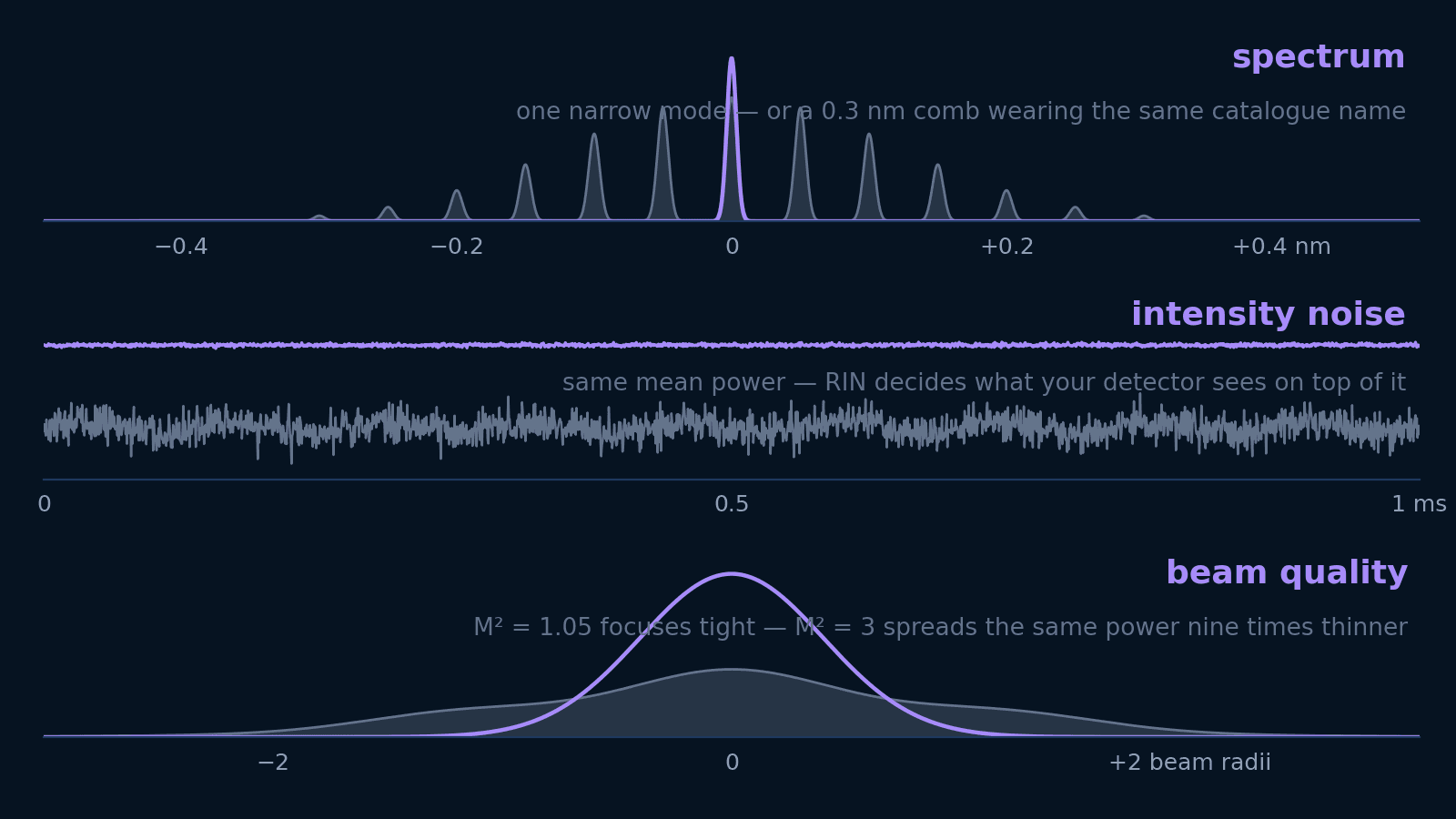
Sweep for spectra; narrow the linewidth for high Q

A broadband tuning range does not guarantee a fine sweep step or a narrow instantaneous linewidth. Those are independent specifications. The catalogue’s 450–2200 nm fibre-coupled tunable source covers the band, but its C-band step and linewidth are not published in the data — ask us before treating it as a resonator source.

Open family
02

Polarization

Set and verify the state at the chip

Use a polarization controller before the DUT and maximize the intended TE or TM response deliberately. If the fibre moves during alignment, recheck the state; alignment and polarization can otherwise masquerade as each other.

Open family
03

Attenuation

Protect the detector and preserve dynamic range

Place a VOA before the device so the search cannot drive the receiver into saturation. Start attenuated, find the optical path, then raise power only as far as the detector and device need.

Open family
04

Routing

Scale from one port to a test sequence

A single device needs no switch. A multi-port PIC, wafer coupon, or regression rack does. Put switching upstream and downstream where it can select paths without disturbing fibre alignment.

Open family
05

DUT

Hold the chip and fibre as one mechanical stack

The coarse and fine stages must share a stiff load path. Build around working distance, fibre approach, chuck clearance, angular access, and the number of ports rather than buying axes in isolation.

Open family
06

Detection

Detect power without hiding the bandwidth

An amplified fibre-coupled photodetector is convenient for DC transmission sweeps. High-speed modulation work may need a different receiver family; bandwidth, gain, saturation, and noise all have to be specified together.

Open family
07

Digitise

Close the loop with a real feedback signal

The control side needs a detector readout, an ADC, and a piezo controller. Precisometer lists a piezo controller and a 20-bit, 100 ksps ADC board that can form the electrical side of an active-alignment loop.

Open family

Packaging and attach

The last alignment move is made by the adhesive.

UV-cure epoxy shrinks as it polymerises and can move the aligned fibre by around a micrometre. That is enough to turn a good edge-coupled measurement into a disappointing package. The coupling did not mysteriously age; the joint pulled it off the peak.

Keep measuring transmitted power throughout the cure and let the fine stage re-optimise, or measure the repeatable cure vector and build compensation into the fixture. Then thermally cycle the joint. Fibre, adhesive, ferrule, package, and chip do not expand by the same amount, and the package has to keep the mode aligned after the station lets go.

The optical test chain

Buy the specification the measurement exposes.

Precisometer already lists the source, conditioning, routing, and detection families for a complete station. The one material catalogue gap is the C-band swept-source specification: tuning coverage exists, but published step and linewidth do not.

Broad tuning coverage for transmission spectra

450-2200nm Tunable Laser Single Mode Fiber Coupled

  • 450–2200 nm coverage in the catalogue title
  • Single-mode fibre coupled
  • C-band step: ask us
  • Instantaneous linewidth: ask us

This is the catalogue route for a swept PIC source, but the two numbers that decide high-Q work — wavelength step and linewidth — are not published in the repository data. Do not buy it for a resonance measurement until those values are confirmed against your device Q.

View catalogue

The narrow-linewidth 1550 nm workhorse

FL-1550-SLM

  • 1550 nm
  • 1–10,000 mW
  • Linewidth <10 kHz or <5 kHz
  • Single-longitudinal-mode fibre laser

Use this when the source linewidth, not sweep range, is the limiting term. It is fixed at 1550 nm, so it does not replace a tunable source; it is the right reference source for a high-Q device or a fixed-wavelength active-alignment loop.

View catalogue

State preparation before a birefringent PIC

Polarization / phase / mode control

  • 16 catalogue products
  • Manual and controlled architectures
  • Use before the VOA and DUT
  • Select to match fibre and wavelength

A polarization controller is mandatory when the coupler or circuit distinguishes TE from TM. The family is deep enough to select an architecture, but product-level wavelength range and connector details still need to match the rest of the chain.

View catalogue

Power control and receiver protection

Fibre optical variable attenuators

  • 22 catalogue products
  • Place upstream of the DUT
  • Start alignment at safe attenuation
  • Match wavelength and connector type

A VOA is cheaper than a saturated detector and safer than searching at full source power. Treat attenuation range, repeatability, return loss, and control interface as application-specific; ask us where the listed product data is incomplete.

View catalogue

Multi-port routing without moving the aligned fibre

Fibre optical switches

  • 104 catalogue products
  • 1×N and matrix routing available in the family
  • Add only when port count justifies it
  • Verify loss and switching architecture per model

Do not insert a switch into a one-port bench merely because it might be useful later; every connector and route adds loss. Add it when automated port coverage or repeated device comparison saves more time than the extra optical path costs.

View catalogue

Plug-and-play readout for transmission sweeps

Fibre-coupled amplified photodetector modules

  • 9 catalogue products
  • Fibre-coupled
  • Amplifier integrated
  • Confirm bandwidth, gain, and saturation per model

Integrated amplification simplifies a slow transmission station. It does not make one receiver universal: a high-speed modulator test and a DC resonance sweep place very different demands on bandwidth and gain.

View catalogue

The positioning stack

Capture with mechanics. Finish with a closed loop.

Coarse XYZ capture range

APFP-XYZ

  • X/Y travel 12 mm
  • Z travel 6 mm
  • Sensitivity <2 µm
  • Manual adjustment

This is a capture stage, not the final alignment axis. Its travel makes setup easy and its published sensitivity is honest about where it stops: a roughly 2 µm manual adjustment cannot reliably sit on a sub-micron coupling peak.

View hardware

Angular acquisition for edge and grating couplers

NFP-2561T / NFP-GON10 / UFP2T

  • NFP-2561T: θy −2° to +4°, θz ±4°
  • NFP-GON10: θx ±10°, sensitivity 6″
  • UFP2T: θx/θy ±3°
  • Choose angle architecture around fibre access

Use the angular stack to establish fibre approach and the grating design angle. Do not use a long angular lever arm to fake fine XYZ: the resulting arc couples translation and rotation and makes an active search harder to interpret.

View hardware

Natural six-degree-of-freedom fine platform

Free6D.3-2.150

  • 6-DOF parallel platform
  • Fine alignment after the manual stage
  • Suitable topology for fibre-to-chip optimization
  • Travel and resolution: ask us

Six controlled degrees of freedom let an optimizer correct the coupled position-and-angle error that a grating probe or multi-axis edge launch produces. The repository confirms the model and topology, not the travel or resolution figures, so those must be matched from the current datasheet.

View hardware

Closed-loop XYZ scanner for the fine axis

S100.XYZ.C

  • XYZ scanner module
  • Closed-loop .C configuration
  • Use inside the coarse stage capture range
  • Exact performance: ask us

Choose this topology when the fibre approach is mechanically fixed and the hard problem is a compact three-axis peak search. Closed loop is the key feature; open-loop hysteresis and creep otherwise turn a repeatable search pattern into a guess.

View hardware

Electrical side of active alignment

Piezo controller + 20-bit / 100 ksps ADC

  • Piezo control hardware
  • 20-bit ADC
  • 100 ksps sampling
  • Control-law integration is application-specific

The controller moves the fine stage and the ADC measures the detector signal that tells it which way is uphill. Sampling speed is ample for a deliberate alignment search; loop dynamics, scaling, interlocks, and software still need to be designed around the selected mechanics and detector.

View hardware

Configure the mechanical stack around the fibre approach.

The fibre-alignment builder is the fastest route from coupling geometry, angular access, and working distance to a compatible coarse positioning stack.

Open the fibre-alignment builder

Common questions

The questions that decide the station.

Why is fibre-to-chip coupling loss so high?

Because the optical modes are radically different sizes. Standard telecom SMF has a mode-field diameter around 10.4 µm, while a bare silicon waveguide mode is well under 1 µm. Gaussian overlap puts the mismatch alone near 20 dB before lateral offset, angle, gap, facet roughness, and Fresnel reflection are counted. A spot-size converter expands the chip mode; a lensed or ultra-high-NA fibre shrinks the fibre mode. Alignment cannot recover power that was lost to mode mismatch, so solve the mode conversion first and specify the stage second.

Should I use edge coupling or a grating coupler?

Use edge coupling when low loss and broad optical bandwidth dominate and you can expose a good facet. Use a grating coupler when top access and wafer-level screening are worth the bandwidth, polarization, and angle constraints. The yield argument is often decisive: a grating lets you measure before dicing and avoid packaging a failed die. Neither is universally better, and the coupling structure should be decided with the test and packaging flow rather than after the mask set is finished.

Do I need active alignment?

For a forgiving grating, a quick screening measurement, or a large expanded edge mode, perhaps not. Vision and manual alignment at roughly 1–2 µm can be enough to enter a broad peak. For a tightly matched edge coupler, repeatable low-loss measurement, long sweeps, or fibre attach, active peak search is the safer choice. It is slower, which is why the practical station uses a coarse manual or vision stage for capture and a closed-loop piezo only for the final search and hold.

What stage resolution does fibre-to-chip alignment need?

Derive it from the one-decibel coupling tolerance, not from a generic nanopositioning rule. A useful search step is about one tenth of that lateral tolerance so the controller samples the peak instead of jumping across it. The interactive coupling lab calculates both values for five coupling schemes. The APFP-XYZ publishes sensitivity below 2 µm and is therefore a coarse stage; when the calculated step is in the tens of nanometres, the final axis needs a closed-loop piezo.

Why does a high-Q resonance drift during a wavelength sweep?

The device temperature is moving the effective index. Around 1550 nm the silicon examples in this guide use a representative resonance shift of 70 pm/K, so a high-Q line can move by a significant fraction of its width while the sweep is still running. Stabilize the chuck, reduce absorbed optical or electrical heating, allow the assembly to settle, and compare wavelength step, source linewidth, and thermal drift independently. A narrower laser does not fix a thermally moving device.

Should I launch TE or TM into the PIC?

Launch the polarization the coupler and circuit were designed for. Most standard one-dimensional silicon grating couplers target TE, but edge couplers and polarization-diverse circuits can be designed differently. Do not infer the state from the fibre connector or the controller setting: maximize the intended device response, document the controller state, and verify extinction against a known polarization-sensitive structure when the measurement needs to be quantitative.

Can I test a PIC at wafer level?

Yes, most directly with surface grating couplers because the fibre approaches from above and no diced facet is required. That turns optical probing into yield screening: test known structures or full devices on wafer, reject poor dies, and reserve dicing and packaging for parts that passed. Wafer-level edge probing also exists, but it requires specialist probes or prepared access and is not the simple default that ordinary butt coupling on a diced die is.

What changes when I permanently attach the fibre?

The alignment becomes a materials and cure-process problem. UV-cure epoxy shrinks and can move the fibre by around a micrometre, enough to leave the coupling peak that looked good before cure. Keep the detector in the loop during attach, re-optimize as the adhesive cures, or design a measured pre-compensation into the fixture. Also check that the cured joint survives thermal cycling without loading the fibre or chip. A good station measurement is not a guarantee of good packaged performance.

Primary sources

  • D. Marcuse, “Loss Analysis of Single-Mode Fiber Splices” (1977). Gaussian mode approximation and the separate loss terms from transverse offset, angular tilt, longitudinal separation, and unequal mode sizes.
  • D. Taillaert, P. Bienstman & R. Baets, “Compact Efficient Broadband Grating Coupler for Silicon-on-Insulator Waveguides” (2004). A standard silicon grating-coupler reference, including TE operation, bandwidth, coupling efficiency, and fabrication tolerance.
  • V. R. Almeida, R. R. Panepucci & M. Lipson, “Nanotaper for Compact Mode Conversion” (2003). The inverse-taper spot-size-converter principle for coupling an optical fibre to a submicrometre silicon waveguide.
  • B. J. Frey, D. B. Leviton & T. J. Madison, “Temperature-Dependent Refractive Index of Silicon and Germanium” (2006). Measured silicon refractive index and thermo-optic coefficient as functions of wavelength and temperature.
  • R. Topley et al., “Erasable Diffractive Grating Couplers in Silicon on Insulator for Wafer Scale Testing” (2014). Why top-access optical test points enable early screening and avoid continuing to process or package known-poor devices.

Send us the platform, coupling scheme, device Q, and port count.

Those four inputs are enough to start sizing the source, polarization and attenuation chain, switching architecture, detector, manual capture range, and closed-loop fine axes. If a catalogue specification is missing, we will ask the manufacturer instead of guessing.

  • Coupling tolerance translated into stage resolution
  • Source linewidth and step checked against device Q
  • Every catalogue gap called out before quotation