Defining the physical inspection envelope
On the factory floor, optical specification always begins at the part surface, not in a catalogue. When an automated inspection station yields unsharp images or fails repeatability tests, the root cause is almost always an overlooked physical constraint rather than a camera sensor defect.
Four governing boundaries dictate what your optical head must physically deliver before camera sensor selection even begins:
Field of View & Part Jitter
The horizontal and vertical area needed to frame the component, inspection features, or alignment fiducials in a single exposure. Critically, this must account for mechanical part-presentation jitter on the fixture; if parts arrive ±1 mm off-center, your field must absorb that tolerance without clipping edges.
Smallest Resolvable Defect
The minimum crack width, solder bridge gap, bond wire diameter, or laser marking dimension that the vision algorithm or operator must reliably discern. Knowing this target dictates whether the active bottleneck will be sensor pixel pitch or optical diffraction.
Working Distance & Clearance
The physical distance between the front mechanical housing of the lens and the in-focus specimen. Tooling needs room for pneumatic part loaders, robotic pick-and-place grippers, and angled illumination heads. In most industrial assembly cells, 75 to 90 mm is the practical sweet spot.
Topography & Height Variation
Component step heights, board warpage, or fixture tilt across the inspection field. Because optical depth of field collapses quadratically with numerical aperture, part topography frequently imposes the governing ceiling on maximum magnification.
Secondary production requirements—such as line throughput (which sets exposure budgets and camera frame rates) and changeover intervals between part variants—determine whether zoom adjustments should be manual, detented for calibration retention, or fully motorized.
Figure 1 · The four primary optical inputs
When a zoom lens is the right optic
Selecting between a fixed machine-vision lens, a telecentric optic, a zoom system, and a microscope turret comes down to how much mechanical and geometrical variability your station must absorb. Each architecture represents a different set of optical trade-offs:
| Optical architecture | Magnification range | FOV changeover | Working distance | DOF / Height variation | Gauging accuracy with height | Typical workstation |
|---|---|---|---|---|---|---|
| Fixed-focal-length lens | < 0.05× to ~0.5× | Fixed (requires lens swap or distance change) | Long (100 mm to > 1 m) | Moderate to deep (set by iris) | Perspective error: apparent size changes with height | Inline presence/absence, packaging, barcode reading |
| Fixed telecentric lens | Single fixed (e.g. 0.5×, 1×, 2×) | None (single field size) | Fixed (typically 40 to 110 mm) | Moderate, highly symmetric | Zero perspective error: constant magnification over DOF | High-speed inline precision dimensional metrology |
| Zoom lens (video-microscope type) | 0.21× to 7.6× continuous | Instantaneous (continuous, detented or motorized) | Moderate (77 to 90 mm) | Deep at low zoom; thin at high zoom | Standard series have perspective; telecentric zoom models eliminate it | Multi-part inspection, rework, QA review, semiconductor packaging |
| Microscope with nosepiece objectives | 2× to 100× discrete | Turret rotation (requires refocusing) | Short to very short (1 to 34 mm) | Very thin (< 0.05 mm) | Not telecentric unless equipped with telecentric tube lens | Failure analysis, metallurgical lab, wafer review |
When an inline station gauges identical stamped pins or turned shafts at high speed and parts never vary, a fixed telecentric lens is usually the cleanest choice. But whenever a cell must inspect multiple board variants, verify different rework zones, or switch smoothly between locating a part at broad field and diagnosing a micro-crack at high magnification—all without touching mounting brackets—a zoom lens provides the necessary flexibility.
Magnification, sensor formats, and image circle matching
With a standard 1× camera tube, object field of view is a direct geometric ratio of physical sensor dimensions to optical magnification:
Geometric scaling, however, is only half the integration challenge. You must also ensure that the lens projects an image circle large enough to cover the active sensor area.
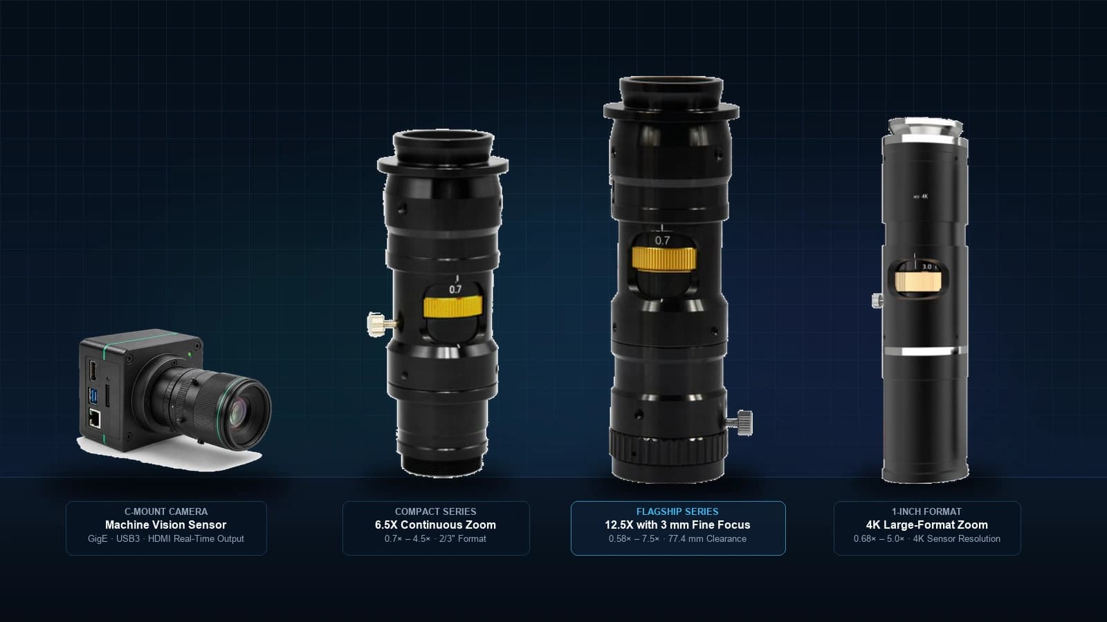
Standard industrial zoom series—including our 12.5X, 14X, and 6.5X product lines—project an 11 mm diameter image circle, sized specifically for 2/3-inch format sensors (8.8 × 6.6 mm, 11.0 mm diagonal). Screwing a 1-inch format camera (16.0 mm diagonal) onto an 11 mm lens causes immediate optical vignetting, casting the corners of your image into total darkness. When working with 1-inch sensors, you must select an optic engineered with a 16 mm image circle, such as our 4K continuous or 6.5X high-resolution series.
Conversely, mounting a smaller sensor—such as a 1/2-inch (6.4 × 4.8 mm) or 1/3-inch format—behind a 2/3-inch zoom lens is optically harmless. There is zero vignetting, but the sensor captures only the central portion of the projected image, cutting your effective maximum field of view by the crop factor.
Figure 2 · One sensor at three optical magnifications
Pixel sampling limits versus optical numerical aperture
When an inspection team needs to isolate a 5 μm solder micro-crack or a 3 μm bond-pad fissure, the instinctive response is often to order a higher-megapixel sensor or screw on a 2× lens extender. On the test bench, this often ends in disappointment. Whether that defect is truly resolvable depends on which of two independent physical ceilings is actively choking your optical train: sensor spatial sampling or optical wave diffraction.
Camera Spatial Sampling Limit
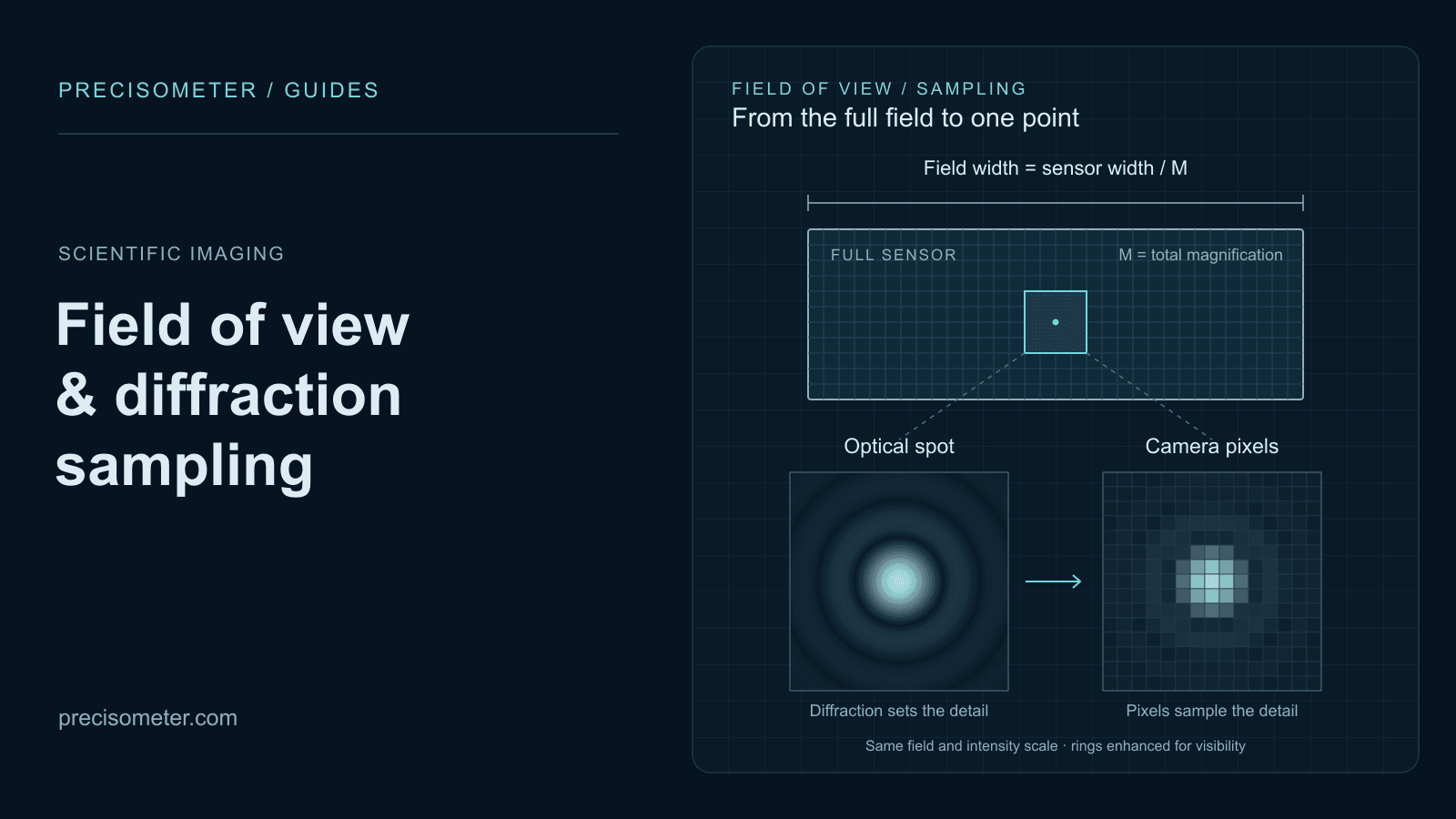
Each sensor pixel projects back into object space as Pixel_size / M. Relying on a single pixel to identify a high-contrast transition produces severe spatial aliasing and unreliable edge segmentation. As Christian Steger, Markus Ulrich, and Carsten Wiedemann formalize in Machine Vision Algorithms and Applications (2018), the Shannon–Nyquist sampling criterion mandates at least two detector pixels across the critical defect dimension:
For industrial edge extraction and sub-pixel fitting algorithms, benchtop reliability typically demands 3 to 4 pixels across the feature.
Optical Rayleigh Diffraction Limit
Regardless of sensor resolution, physical wave optics imposes an uncompromising ceiling governed by numerical aperture (NA) and light wavelength (λ = 0.55 μm for visible green). As Warren J. Smith outlines in Modern Optical Engineering (2008), the classic Rayleigh criterion defines the minimum resolvable separation between two Airy disks:
Across a zoom stroke, NA is dynamic: on our 12.5X series, NA scales from 0.025 at 0.58× (13.4 μm resolution) up to 0.110 at 4.5×–7.5× (3.05 μm resolution).
The 2.2× Crossover & Empty Magnification
Understanding this boundary explains a classic lab frustration. On a standard machine vision camera with 3.45 μm pixels, the sensor sampling curve and the optical diffraction curve intersect at roughly 2.2× optical magnification. Below 2.2×, pixel pitch is the true bottleneck: zooming in reveals genuine surface microstructure. Past 2.2×, optical diffraction takes over. Turning the zoom collar from 3× up to 7.5× merely magnifies Airy disks across more pixels without resolving smaller physical features.
This condition—termed empty magnification in classical optics literature (Inoué & Spring, Video Microscopy, 1997)—narrows your field of view and starves your sensor of photons without uncovering smaller flaws. If your station requires resolving features below 3 μm, higher zoom magnification won't help; you need higher numerical aperture objectives or shorter-wavelength illumination.
Figure 3 · Camera pixel limit vs optical resolution limit
Depth of field and working clearance
While lateral resolution improves linearly with numerical aperture, depth of field decays quadratically:
The practical consequence on the factory floor is severe. On our 12.5X flagship series, depth of field shrinks from a generous 2.75 mm at 0.58× zoom down to barely 0.05 mm (50 μm) at 7.5× zoom. A 0.4 mm stepped capacitor, a slightly bowed PCB substrate, or minor mechanical runout on a rotating fixture will look crisp across the entire field at 1× zoom, yet blur into illegibility as soon as you zoom in to inspect a terminal lead.
Engineering strategies for stepped or non-flat specimens
When part topography exceeds optical depth of field, experienced machine vision engineers employ several practical benchtop workarounds:
Trading optical magnification for smaller sensor pixels
When vertical clearance is tight, consider holding optical magnification lower (say 1.0× to 1.4×) and moving to a sensor with smaller physical pixels (such as 2.4 μm or 2.74 μm) rather than cranking the zoom barrel. You preserve your millimetre-scale depth of field while gaining digital sampling density.
Fine-focus mechanical collars on manual benches
When inspecting varied boards on a rework station, repeatedly unbolting and adjusting a heavy boom stand or focus block is clumsy and invites vibration. A lens barrel with an integrated fine-focus collar (available with 3 mm or 12 mm axial travel) lets technicians tune focal planes with a light fingertip rotation, leaving the main rig untouched.
Motorized Z-stepping and focus stacking
In automated cells with tall components, motorized focus barrels or precision motorized Z-stages execute stepped image bursts across focal layers. Vision software then computationally fuses the in-focus regions into an extended depth-of-field (EDOF) composite.
Working distances in the catalogue remain constant across zoom on standard models (77.4 ± 2 mm for 12.5X; 80 mm for 14X; 86 mm for 4K; 88 mm for 6.5X HR; 90 mm for 6.5X), providing a stable mechanical envelope for robotic grippers and illumination brackets.
Illumination geometry and mechanical drive architectures
As B.G. Batchelor underscores in the Machine Vision Handbook (2012), no optical assembly or image-processing algorithm can compensate for defective illumination geometry. The mechanical housing and optical layout of a zoom lens must match both the surface reflectance of the specimen and the operational demands of the production line.
Coaxial Illumination for Specular Surfaces
Inspecting polished silicon wafers, IC bond pads, glass substrates, or mirrored metal stampings with standard external ring lights causes severe glare, blinded camera regions, and shadow occlusions.
Coaxial zoom models integrate an internal beam splitter prism directly within the optical barrel, directing light normal to the workpiece along the optical axis. Perpendicular reflections return straight to the sensor, rendering metallization and polished pads crisp and bright while scattering unpolished surface defects as dark features.
For diffuse, matte, or textured parts, external low-angle darkfield illuminators, multi-angle diffuse ring lights, or backlights are preferred.
Mechanical Drive Architectures
Interactive tool: Inspection Optics Planner
Use the planner below to test your inspection constraints. All calculations assume a standard 1× adapter tube and derive resolution and depth of field directly from published optical tables:
Interactive engineering tool
Inspection Optics Planner
Compute object-space pixel size, Rayleigh optical resolution limit, depth of field, and the feasible magnification window for any camera and zoom lens in the catalogue.
Every preset is an illustrative set of numbers, not the performance of any detector, source or instrument.
WD: 77.4 ± 2 mm · Max sensor: 2/3 inch
Diagonal: 11.0 mm (Covers sensor)
Common: 3.45 µm (Sony Pregius), 2.4 µm, 5.5 µm
Defect size or minimum line width to detect
2 px is theoretical minimum; 3–4 px ensures robust segmentation.
Step height, component tilt, or Z tolerance
Continuously variable within 12.5X zoom lens range (0.58× to 7.5×)
Feasible magnification window: 0.79× to 1.38×
Inside this range, the full 4 × 3 mm field fits on the sensor, resolvable detail is ≤ 10 µm, and depth of field covers the 0.5 mm height step. depth of field, not field of view, caps the magnification here.
Synchronized Optical Trade-Off Plots
Hover or use arrow keys across any plot to inspect values. Shaded zone shows feasible window. Click or press Enter to set operating magnification.
Next step: Hardware pairing
Find cameras and versions in the selector
Take these field-of-view and resolution numbers directly into our interactive selector. It tests our full camera range against the 12.5X zoom lens and ranks matching configurations.
Quotation & engineering review
Send these numbers to Precisometer
Send our optics engineers your part dimensions, smallest defect and working clearance. We will verify the mechanical envelope, propose lens attachments, and send an itemized quotation.
Planner optics formulas and calculation assumptions
1× Adapter Tube Baseline: All fields of view, resolutions and depths of field are evaluated for a standard 1× TV camera adapter tube with no auxiliary front lens attachment. Auxiliary attachments (e.g. 0.5× or 2.0×) scale magnification, working distance and numerical aperture accordingly.
Resolution Criterion: Optical resolution follows the Rayleigh diffraction limit at green wavelength (λ = 0.55 µm): r = 0.61 λ / NA. The camera sampling limit is d_cam = (N_px × p) / M, where p is sensor pixel pitch and N_px is the requested pixels across the feature (minimum 2 by the Nyquist–Shannon theorem). The overall limit is the coarser of the two: max(d_lens, d_cam).
Depth of Field (DOF): Values are derived from the published optical tables of each zoom lens series, using log-log interpolation between measured magnification points. Depth of field scales approximately as 1/NA².
Illustrative Nature: Every scenario and calculation in this tool is illustrative and based on published datasheet specifications. Real-world defect contrast also depends on illumination geometry, part reflectance, camera quantum efficiency, and optical surface finish.
Benchtop Feasibility Walkthrough: SMT Component & Fillet Inspection
Worked Engineering CheckConsider a typical production station setup: a quality engineer must inspect 0402 chip components and solder fillet wetting on a crowded board. The station parameters are:
1. Framing constraint: To fit the 4.0 × 3.0 mm inspection area onto the 8.8 × 6.6 mm sensor, the maximum magnification based on field of view is min(8.8 / 4.0, 6.6 / 3.0) = 2.20×.
2. Resolution check at 2.20×: Object-space pixel size is 3.45 μm / 2.20 = 1.57 μm, yielding a 2-pixel camera sampling limit of 3.14 μm. Optical diffraction at 2.20× is 4.34 μm. Both comfortably beat the 10 μm defect threshold.
3. The depth of field trap: At 2.20×, optical depth of field drops to 0.238 mm. This is less than half the 0.50 mm component height step. Running the station at 2.20× would leave tall component bodies or board steps severely out of focus.
4. Viable operating window: Resolving the 10 μm crack requires at least 0.78× magnification (lens limited). Maintaining 0.50 mm depth of field caps magnification at 1.39×. The viable operating window is 0.78× to 1.39×.
5. Station configuration: Locking the lens at 1.39× delivers an object field of 6.34 × 4.75 mm, an optical resolution of 5.7 μm, and exactly 0.50 mm depth of field—clearing the full component height while resolving 10 μm cracks.
Three verified benchtop configurations
The following three case studies demonstrate how catalog optical specifications translate into robust, repeatable inspection systems across different manufacturing environments:
SMT solder joint and 0402 component inspection
Benchtop Challenge
Inspect 0402 chip passives, solder fillet wetting, and lead bridging across a 4 × 3 mm area. The station must resolve 10 μm cracks while clearing tall adjacent capacitors and tolerating slight board warpage without continuous refocusing.
Optical Solution
12.5X Zoom Lens with 3 mm Fine Focus. The 77.4 ± 2 mm working distance leaves ample clearance for an angled diffuse LED ring light. The integrated 3 mm fine-focus collar accommodates warped boards without unbolting or adjusting the main boom stand.
Verified Operating Parameters (at 1.39× zoom):
Sensor: 2/3-inch (8.8 × 6.6 mm, 3.45 μm pixels)
Field of view: 6.34 × 4.75 mm
Optical resolution: 5.7 μm (diffraction limited)
Depth of field: 0.50 mm (clears component height step)
Polished silicon die and wire-bond defect review
Benchtop Challenge
Inspect polished silicon wafer die, bond pads, and evaporated metallization traces. High specular reflectance creates blinding glints and deep shadow artifacts when illuminated with standard external ring lights.
Optical Solution
12.5X Zoom Lens with Coaxial Illumination. An integrated coaxial beam splitter introduces perpendicular illumination straight down the optical axis, turning the flat mirror die bright while defects scatter light and show up dark.
Verified Operating Parameters (at 4.0× zoom):
Sensor: 2/3-inch (8.8 × 6.6 mm, 3.45 μm pixels)
Field of view: 2.20 × 1.65 mm
Lens resolution: 3.36 μm (NA 0.10)
Depth of field: 0.10 mm (100 μm)
Non-contact dimensional gauging of stepped turned components
Benchtop Challenge
Measure pin diameters and stepped hole positions where parts have up to 1.5 mm of axial height variation. Standard entocentric lenses produce perspective distortion, causing features closer to the lens to appear larger and corrupting measurement tolerances.
Optical Solution
Telecentric Zoom Lens, 0.21× to 1.97×. True object-space telecentricity (< 0.05°) guarantees that magnification remains constant throughout the entire depth of field, eliminating perspective error.
Verified Operating Parameters (at 0.5× zoom):
Sensor: 1-inch format (12.8 × 9.6 mm)
Object field: 25.6 × 19.2 mm
Optical resolution: 10.64 μm (NA 0.034)
Depth of field: 1.18 mm (geometric distortion 0.06%)
Planning an inspection station?
Every machine vision station is a trade-off between field size, sensor pixel pitch, working clearance, and vertical depth of field. Send us your component specifications, defect thresholds, and mechanical envelope, and our optical team will configure the exact zoom body, camera sensor format, and illumination pairing for your line.
Inspection station specification checklist
- Part description and material (reflective metal, matte polymer, silicon, PCB)
- Smallest feature or defect to resolve (µm)
- Required field of view: width × height (mm)
- Working distance and mechanical clearance above the station (mm)
- Part height variation or step thickness (mm)
- Camera choice: existing model or "please propose camera"
- Illumination type (coaxial for specular parts, ring light, low-angle darkfield, backlight)
- Zoom drive mode (manual continuous, detented for calibration retention, motorized for automation)
- Fine focus requirement (fixed, 3 mm fine focus, 12 mm fine focus, motorized focus)
- Output interface (USB3 / GigE / CoaXPress to PC, or direct HDMI to monitor)
- Estimated quantity and project timeframe
Cited technical references
- • Steger, C., Ulrich, M., & Wiedemann, C. (2018). Machine Vision Algorithms and Applications (2nd ed.). Wiley-VCH.
- • Batchelor, B. G. (Ed.). (2012). Machine Vision Handbook. Springer.
- • Smith, W. J. (2008). Modern Optical Engineering: The Design of Optical Systems (4th ed.). McGraw-Hill.
- • Inoué, S., & Spring, K. R. (1997). Video Microscopy: The Fundamentals (2nd ed.). Plenum Press.