Architecture Explainer
CCD vs CMOS: Readout Architectures & Physics
How an image sensor physically moves photoelectrons and converts charge into digital counts dictates its readout speed, read noise floor, spatial uniformity, and dynamic range.
The Core Split
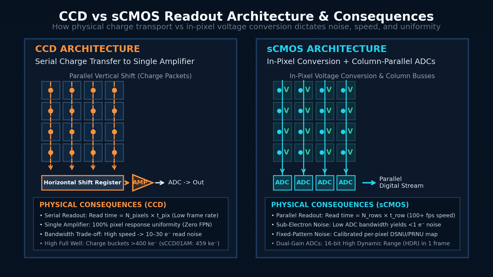
CCD shifts charge packets across silicon to a single corner amplifier. CMOS converts charge to voltage at every pixel and reads in parallel.
Speed vs Read Noise
Single CCD amplifier demands high bandwidth -> 10–30 e⁻ noise. Parallel sCMOS column ADCs run at narrow bandwidth -> sub-electron (<1 e⁻) noise at 100+ fps.
Why CCD Survives
Zero amplifier fixed-pattern noise and massive full well capacity (>400 ke⁻) preserve CCD dominance in long-exposure spectroscopy.
The architecture in one sentence
CCD moves charge to a single amplifier; CMOS converts charge to voltage at every pixel.
Every imaging specification on a camera datasheet — from frame rate and read noise to response non-uniformity, blooming, and shutter behavior — is a direct physical consequence of this fundamental topological split.
While our companion guide Choosing a Scientific Camera focuses on the buyer’s decision framework (photon budget → technology → shutter → interface), this page explains the underlying device physics: how silicon charge movement dictates performance limits.
CCD Transport
Charge packets march physically across silicon pixels into a corner register and a single output node.
CMOS Parallelism
Active in-pixel transistors convert charge to voltage; column busses stream full rows to dedicated ADCs.
Downstream Impact
Parallel readout lowers amplifier bandwidth -> sub-electron noise. Single amplifier preserves raw response uniformity.
1 · Core architectural split
Charge transfer through silicon versus in-pixel voltage conversion.
Physical Charge Transport
In a CCD (Charge-Coupled Device), pixels consist of MOS capacitors formed directly in high-resistivity silicon. During exposure, incident photons create electron-hole pairs, and photoelectrons are trapped in potential wells.
To read out the image, clock voltages applied to gate electrodes manipulate the potential wells, shifting charge packets down vertical columns into a horizontal shift register. The register then transfers charge packets one-by-one to a single sense node capacitor connected to a corner output amplifier.
In-Pixel Voltage Conversion
In a CMOS image sensor, charge is converted to voltage directly inside every individual pixel. Modern 4T (four-transistor) active pixel sensors incorporate a pinned photodiode, a transfer gate, a floating diffusion node, a reset transistor, and a source-follower amplifier inside each pixel boundary.
Instead of moving charge across the chip, pixel voltages are selected row-by-row and driven down vertical column lines to an array of hundreds or thousands of column-parallel Analog-to-Digital Converters (ADCs) operating simultaneously.
2 · Downstream consequences
What follows from the topology: noise, speed, power, and uniformity.
Choosing how charge is read out dictates every performance trade-off in the image detector chain.
Charge-to-Voltage Conversion Location
Off-chip / corner node: Charge packets are physically moved across silicon into a single output capacitor.
In-pixel: Every pixel contains 3 or 4 active transistors converting charge to voltage directly at the photodiode.
Readout Parallelism & Speed
Serial: T_read = N_pixels × t_pix. Megapixel arrays require seconds to read out at low noise levels.
Massively Parallel: T_read = N_rows × t_row. Busses stream whole rows into per-column ADCs simultaneously (100+ fps).
Read Noise Mechanism
Single amplifier must run at high pixel clock bandwidth (10–30 MHz) -> 10–30 e⁻ rms read noise.
Per-column ADCs run at narrow bandwidth per channel -> sub-electron read noise (<1.0 e⁻ rms in sCMOS HDR).
Pixel Response Uniformity
Near 100% uniform: All charge packets pass through the exact same output amplifier (Zero amplifier FPN).
Requires calibration: Millions of distinct in-pixel transistors and column ADCs produce Fixed-Pattern Noise (FPN).
Full-Well Capacity & Bucket Size
Very Large: Deep charge buckets (>400 ke⁻ per pixel in line sensors like sCCD01AM).
Moderate: In-pixel transistor real estate limits charge node storage (~30–50 ke⁻ in standard sCMOS pixels).
Over-exposure Behavior
Blooming & Smear: Excess charge spills along vertical transfer channels into adjacent rows.
No Smear: Photodiodes are electrically isolated; over-exposed pixels cannot ruin unexposed rows during readout.
Fixed-Pattern Noise (FPN) & Calibration
Because a CCD reads every charge packet through the exact same output amplifier, pixel-to-pixel gain and offset variations are virtually non-existent. A CMOS sensor, by contrast, relies on millions of distinct in-pixel source-follower transistors and hundreds of column ADCs. Minute silicon threshold variations create Fixed-Pattern Noise (FPN). Scientific sCMOS cameras solve this using embedded FPGA hardware that applies pixel-by-pixel Dark Signal Non-Uniformity (DSNU) and Photo Response Non-Uniformity (PRNU) correction maps in real time.
Blooming, Smear & Over-exposure
In a CCD, pixels in the same column share potential wells during shift readout. If a bright spot overfills a pixel well, excess charge spills along the vertical channel, creating vertical bright streaks (“blooming”). Furthermore, light falling on the chip while charge is shifting creates vertical readout “smear”. CMOS pixels isolate charge in-pixel and stream voltages down dedicated busses; over-exposed pixels cannot contaminate adjacent rows during readout.
3 · Shutter physics
Rolling shutter is a CMOS consequence, not a design oversight.
Understanding why CMOS sensors default to rolling shutter requires examining the physical silicon layout of active pixel structures.
Standard 4T Rolling Shutter Pixel
A high-performance sCMOS pixel uses a 4-transistor (4T) architecture to maximize light-collecting photodiode area (fill factor) and minimize read noise. However, because column ADCs are shared across all rows, the sensor must reset and read out row-by-row sequentially. Row 1 begins exposure slightly before Row 2, producing a rolling temporal window down the frame.
5T / 6T In-Pixel Global Shutter
To capture all pixels at the exact same instant, a Global Shutter CMOS pixel adds an additional in-pixel memory storage node and transfer gate (5T or 6T design). Charge accumulates simultaneously across all photodiodes, then transfers into shielded in-pixel memory nodes at the exact same moment.
4 · Illumination & fill factor
Front- versus back-illumination and micro-lens arrays.
Light through Metal Wiring Layers
In a Front-Illuminated sensor, incident light passes through dielectric and metal interconnect layers (metal busses, gate electrodes) before reaching the photosensitive silicon layer underneath. Metal lines reflect or absorb incoming photons, reducing the effective fill factor. Micro-lenses are placed over each pixel to focus light into the open photodiode aperture, limiting peak Quantum Efficiency (QE) to ~60–75%.
Direct Silicon Exposure (95% Peak QE)
In a Back-Illuminated (BSI) sensor, the silicon wafer is flipped upside down during manufacturing and mechanically ground/chemically etched down to a thickness of ~10 µm. Light enters directly through the back silicon surface without encountering metal wiring obstacles. 100% of the pixel area is sensitive to photons, driving peak Quantum Efficiency to 95% (e.g. sMAX04BM at 560 nm).
5 · Scientific CMOS (sCMOS)
What separates scientific CMOS from consumer phone sensors.
Commercial smartphone sensors prioritize miniature pixel pitch (e.g. 0.8 µm) and low cost. Scientific CMOS (sCMOS) redesigns the column readout architecture for quantitative physics and biology.
Dual-Gain Column Amplifiers
Each column contains both a High Conversion Gain (HCG) amplifier for sub-electron noise in low light and a Low Conversion Gain (LCG) amplifier for high full-well headroom. Both channels are digitized simultaneously to synthesize 16-bit High Dynamic Range (HDR) images in a single frame.
Correlated Multiple Sampling (CMS)
By sampling the pixel reset level and signal level multiple times per conversion cycle, high-frequency reset noise (kTC noise) is mathematically cancelled before column ADC output, enabling sub-electron rms noise floors.
Back-Illuminated (BSI) Processing
Silicon wafers are inverted and mechanically thinned to ~10 µm, exposing photodiodes directly to incident light without wiring attenuation — boosting peak quantum efficiency from ~65–70% (FSI) to 95%.
Real Catalog Proof: sMAX04BM Dual Readout Modes
On the sMAX04BM (GSENSE2020BSI), the dual-gain column architecture allows switching readout modes depending on photon flux:
• HDR 11HL Mode: 0.97 e⁻ rms read noise for single-molecule fluorescence.
• 12-bit LCG Mode: 23.25 e⁻ read noise with expanded 54 000 e⁻ full-well capacity for bright signal imaging.
6 · Why CCD survives
Full well capacity, zero amplifier FPN, and long exposures.
CCD is neither obsolete nor replaced across all applications. Understanding where CCD retains physical superiority prevents costly mis-specifications.
Massive Charge Buckets
Without in-pixel transistors occupying silicon area, CCD pixels can store enormous charge quantities. The sCCD01AM (E2V CCD261 linear CCD) features a 459 000 e⁻ full-well capacity per pixel — more than 10× that of typical sCMOS pixels.
Single-Amplifier Precision
In spectroscopy lines, subtle spectral line shapes cannot tolerate spatial gain variations introduced by multi-channel column ADCs. CCD passes all spectral channels through a single output amplifier, preserving uncalibrated physical response linearity.
Long-Exposure Photometry
Deep TE cooling (55 °C below ambient on sCCD01AM to reach -35 °C) reduces dark current to 184 e⁻/px/s even across large binned pixels. For multi-minute astronomical exposures or Raman spectroscopy, dark noise control and full well beat frame rate.
7 · Architecture lab
Simulate CCD vs sCMOS readout physics in real time.
Select real camera models from our catalog, set incident photon flux and exposure duration, and observe how read noise, shot noise, dark current, full well capacity, and readout speed interact across different sensor architectures.
Readout Architecture Simulator
CCD vs sCMOS Readout Physics Lab
sMAX04BM (Sub-electron sCMOS - HDR Mode)
- Incident Photons / Frame
- 50 e⁻ equiv
- Signal Electrons (QE 95%)
- 47.5 e⁻
- Read Noise (N_r)
- 0.97 e⁻ rms
- Full Well Capacity
- 30,000 e⁻
- Dynamic Range per Frame
- 30,928:1 (89.8 dB)
- Max Frame Rate / Read Time
- 108 fps (9.3 ms/frame)
Readout Topology:
Parallel (In-pixel 4T charge-to-voltage + per-column dual ADCs)
★ Requires factory per-pixel gain & offset calibration (FPN map)
sCCD01AM (Deep-cooled Scientific Line CCD)
- Incident Photons / Frame
- 50 e⁻ equiv
- Signal Electrons (QE 95%)
- 47.5 e⁻
- Read Noise (N_r)
- 22 e⁻ rms
- Full Well Capacity
- 459,000 e⁻
- Dynamic Range per Frame
- 20,864:1 (86.4 dB)
- Max Frame Rate / Read Time
- 12 fps (83.3 ms/frame)
Readout Topology:
Serial (Parallel vertical shift into horizontal shift register -> 1 output amp)
★ 100% physical response uniformity (zero amplifier FPN)
Physical Takeaway from this Simulation
sMAX04BM (Sub-electron sCMOS - HDR Mode) achieves significantly higher SNR in this photon flux regime. Because read noise is squared in the noise equation (Nr²), 0.97 e⁻ vs 22 e⁻ makes an enormous difference when photon count is low.
8 · Honest 2026 verdict
Where each sensor architecture wins in 2026.
We avoid simple dogmatism: CCD is not obsolete, and sCMOS is not a universal panacea. Here is where the physics stands today.
Where sCMOS Wins (95% of Use Cases)
- Low-Light Fluorescence & Single-Molecule: Sub-electron read noise (<1.0 e⁻) coupled with 95% BSI QE provides unmatched SNR when photon flux is under ~100 photons/pixel.
- High-Speed Dynamics & Live Cells: Column-parallel readout delivers 100+ fps full-frame megapixel rates impossible on CCD without prohibitive noise penalty.
- Single-Frame High Dynamic Range: Dual-gain column amplifiers digitize high and low conversion gain simultaneously for 16-bit HDR.
Where CCD Wins
- High-Signal Spectroscopy & Line Scans: Massive full well capacity (>400 ke⁻ per pixel in sCCD01AM) allows accumulating high signal without saturating channels.
- Absolute Photometric Uniformity: Single-amplifier charge transport eliminates column fixed-pattern noise (FPN) artifacts across uncalibrated raw frames.
- Long-Exposure Astronomy & Deep Raman: When exposure durations exceed minutes, deep cooling (-35 °C) and large binned buckets outperform rapid-frame CMOS averaging.
9 · Products
Featured detectors in our scientific catalog.
Every figure quoted below is drawn directly from our catalog specifications. Promote sCMOS for speed and low noise; select CCD when full-well capacity and line spectroscopy dictate.
sMAX04BM-CL100
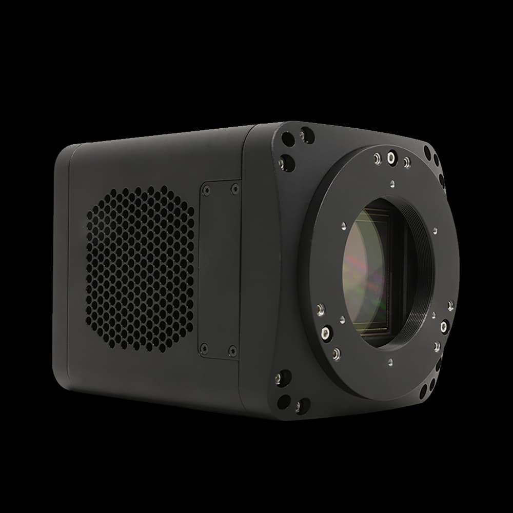
The GSENSE2020BSI 4.2 MP back-illuminated sCMOS platform. In HDR 11HL mode it achieves 0.97 e⁻ rms read noise and 95% peak QE @ 560 nm at up to 108 fps full frame over Camera Link. Represents the modern gold standard for fluorescence and quantitative scientific imaging.
sCCD01AM
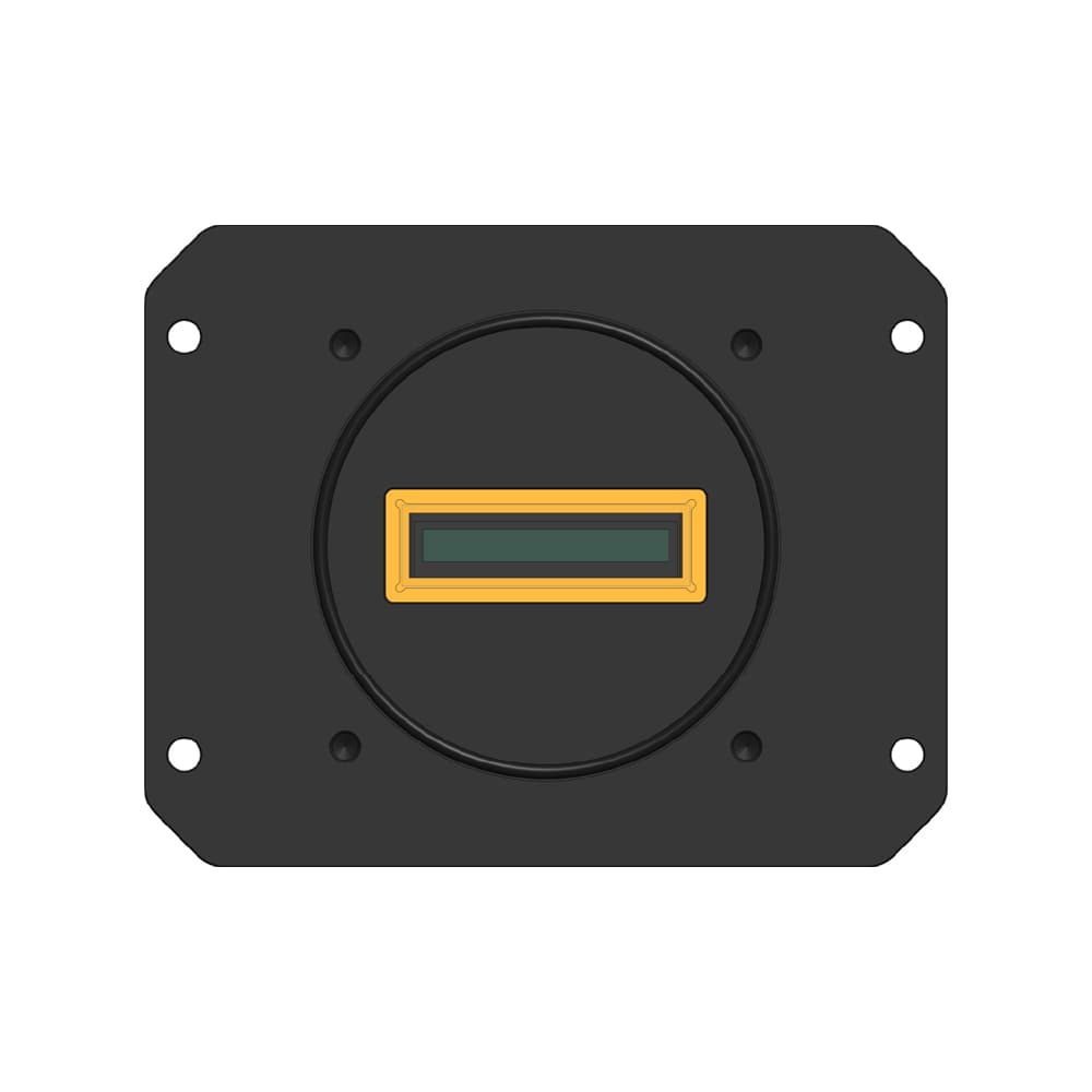
A deep-cooled 2048 × 1 E2V CCD261 linear detector featuring a massive 459 ke⁻ full well capacity and 95% QE @ 800 nm with 184 e⁻/px/s dark current @ -35 °C. When a spectrum contains 100 000 photoelectrons per channel, CCD response uniformity and full-well capacity beat sCMOS.
sMAX16BM-U3-CL
A 16.8 MP GSENSE4040BSI sensor on a 36.9 mm square format. Delivers 90% peak QE @ 550 nm and 9 µm pixels for large field-of-view quantitative microscopy, replacing complex tiling stages with single-frame acquisition.
10 · Related guides
Explore decision frameworks and specialized sensor technologies.
Choosing a scientific camera
Photon budget, noise regimes, shutter selection, and interface bandwidth checks before making a purchasing decision.
Open guide sCMOS In DepthHow to select an sCMOS camera
Compare quantum efficiency, read-noise modes, pixel size, and optical sampling across real sMAX specifications.
Open guide Beyond SiliconWhen silicon isn't enough: choosing a SWIR camera
Why silicon detectors stop at 1100 nm, InGaAs focal plane architectures, dark current, and SWIR cooling.
Open guide11 · Common questions
Frequently asked questions about CCD vs CMOS sensor physics.
How do CCD and CMOS image sensors physically differ?+
The fundamental difference is where charge-to-voltage conversion takes place. In a CCD (Charge-Coupled Device), accumulated photoelectron packets are physically shifted row-by-row and column-by-column across the silicon array into a single output node at the corner of the chip. In a CMOS sensor, every pixel contains active transistors (3T or 4T architecture) that convert charge into a voltage signal directly at the photodiode site, streaming voltages down column busses to parallel Analog-to-Digital Converters (ADCs).
Why is sCMOS so much quieter and faster than CCD?+
Read noise scales directly with amplifier bandwidth. Because a CCD routes all pixels through a single output amplifier, that amplifier must operate at multi-megahertz clock rates (e.g. 10–30 MHz) to deliver even modest frame rates, resulting in 10–30 e⁻ rms read noise. sCMOS uses thousands of parallel per-column ADCs running simultaneously at very low individual sampling bandwidths, which lowers the amplifier noise floor down to sub-electron levels (<1.0 e⁻ rms) while delivering 100+ frames per second.
Why does CCD still win in long-exposure spectroscopy?+
CCD pixels do not contain in-pixel transistors, leaving almost the entire pixel area available as a deep silicon charge bucket (>400 ke⁻ full well in line CCDs like sCCD01AM, versus ~30 ke⁻ in standard sCMOS pixels). Furthermore, because every pixel in a CCD reads through the exact same amplifier, response non-uniformity (PRNU) across the array is virtually zero without requiring complex digital correction. For spectroscopy or astronomical photometry where high photon counts are accumulated over long exposures, CCD full-well headroom and raw spatial uniformity remain superior.
Why is rolling shutter a natural consequence of CMOS?+
In a basic 4T sCMOS pixel, charge accumulates in the photodiode until read out row-by-row. Because the readout circuitry is located at column ends rather than inside every pixel, rows must be reset and read sequentially in time, producing a rolling shutter effect. Achieving a true global shutter in CMOS requires adding an extra shielded storage transistor inside every individual pixel (5T or 6T pixel structure), which reduces fill factor, light-collecting area, and full-well capacity relative to a rolling-shutter pixel on the same process.
What is Fixed-Pattern Noise (FPN) and why does it affect CMOS more than CCD?+
Because every CMOS pixel has its own amplifier transistors and every column has its own ADC, minute microscopic manufacturing variations produce slight offset and gain differences between pixels and columns. This manifests as Fixed-Pattern Noise (FPN). Modern scientific sCMOS cameras eliminate FPN using precision real-time factory calibration maps (DSNU and PRNU corrections) loaded into camera FPGA hardware.
What makes "sCMOS" different from a standard CMOS smartphone or industrial camera?+
Scientific CMOS (sCMOS) incorporates specific physical architectures absent in consumer sensors: dual-gain column amplifiers (simultaneously reading High Conversion Gain for low noise and Low Conversion Gain for capacity to produce 16-bit HDR images), Correlated Multiple Sampling (CMS) to eliminate reset noise, deep thermoelectric cooling to reduce dark current, and back-illuminated (BSI) wafer processing for 95% peak quantum efficiency.
What are blooming and smear in CCD sensors?+
In a CCD, pixels share physical vertical charge transfer channels. When a pixel receives light beyond its full-well capacity, excess photoelectrons overflow along the vertical transfer channel into adjacent rows, creating vertical bright streaks ("blooming"). During frame readout while light is still falling on the sensor, shifting charge through bright regions creates vertical "smear". CMOS sensors do not shift charge across columns, eliminating readout smear entirely.