RTS-miniRaman Confocal Spectrometer
Micro-Raman measurement and mapping on the upright microscope you already have.
A compact excitation and collection module, a 320 mm Czerny-Turner spectrograph and one of three excitation lines. Supplied with a microscope, or fitted to yours.
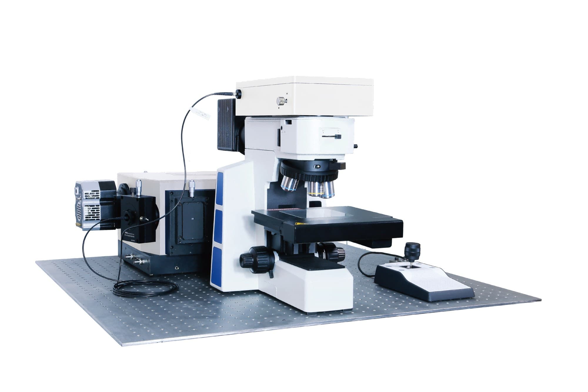
System
RTS-mini on an Upright Microscope
Excitation and collection module mounted above the microscope head, fibre-coupled to the 320 mm spectrograph and CCD. Supplier branding removed from the public render.
System Highlights
Research-Grade Raman in a Small Footprint
The RTS-mini keeps the parts that decide data quality — excitation line, spectrograph, gratings and confocal collection — and leaves the microscope choice to you.
Couples to Most Upright Microscopes
The Raman module attaches to the trinocular port of most upright microscopes. Supply your own microscope, or take the system complete with one.
532, 638 or 785 nm Excitation
Order the excitation line around the samples: 532 nm for the widest shift range, 638 nm as a middle ground, 785 nm where fluorescence has to be suppressed.
Low-Wavenumber Reach
80 cm⁻¹ typical and 100 cm⁻¹ guaranteed in a compact system — the lattice and layer-breathing region stays accessible without a triple monochromator.
Raman Mapping
Add the motorised stage option and record a spectrum at every point of a grid. Graphene and MoS₂ flakes were mapped at 0.5 µm step with a 50× objective.
320 mm Czerny-Turner Spectrograph
Three blazed gratings per excitation line let you trade resolution against spectral window; < 1.5 cm⁻¹ at 532 and 638 nm, 2.3 cm⁻¹ at 785 nm.
Non-Destructive, Minimal Preparation
Polymers, ceramics, nanomaterials and 2D materials such as graphene or monolayer MoS₂; blood, tissue and cells with a suitable excitation wavelength.
System Performance
Three Numbers, Each Backed by a Measured Spectrum
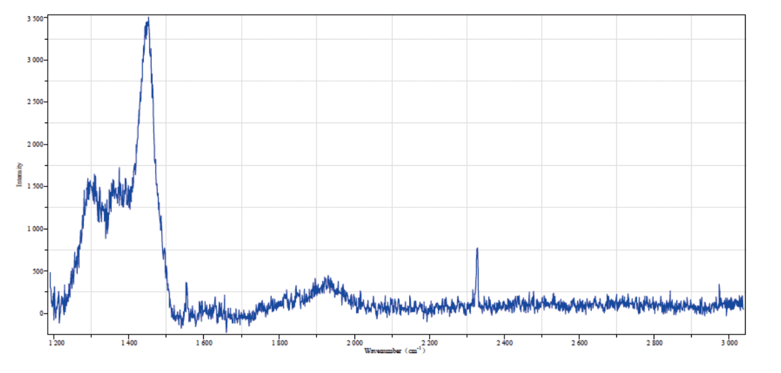
Third-Order Raman Peak of Monocrystalline Silicon
The weak third-order band near 1450 cm⁻¹ is the standard sensitivity check; recorded at S/N > 20:1.
Excitation Options
One Laser Line, Chosen for the Sample
Each RTS-mini is built around a single excitation wavelength with a matched set of three blazed gratings. Not sure which line suits your samples? The excitation wavelength guide works through signal strength, fluorescence and spectral window.
Strongest Raman signal and the widest shift range; the default for inorganic, 2D and carbon materials.
- Laser power
- 100 mW
- Raman shift range
- 80–9000 cm⁻¹
- Spectral resolution
- 1.5 cm⁻¹
Grating options
- 1800 g/mm, 500 nm blaze
- 600 g/mm, 500 nm blaze
- 150 g/mm, 500 nm blaze
Less fluorescence than 532 nm at a smaller efficiency penalty than 785 nm.
- Laser power
- 50 mW
- Raman shift range
- 80–6000 cm⁻¹
- Spectral resolution
- 1.5 cm⁻¹
Grating options
- 1200 g/mm, 750 nm blaze
- 600 g/mm, 750 nm blaze
- 150 g/mm, 750 nm blaze
Suppresses fluorescence from polymers, pharmaceuticals and biological samples.
- Laser power
- 100 mW
- Raman shift range
- 80–3200 cm⁻¹
- Spectral resolution
- 2.3 cm⁻¹
Grating options
- 600 g/mm, 750 nm blaze
- 300 g/mm, 750 nm blaze
- 150 g/mm, 750 nm blaze
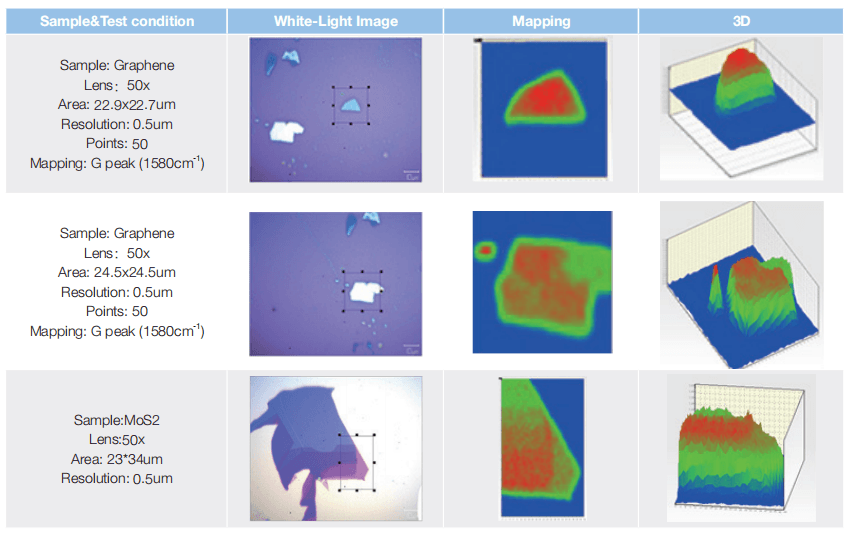
Raman Mapping
From White-Light Image to Chemical Map
With the motorised stage option the software records a spectrum at every point of a user-defined grid and plots the intensity of a chosen band as a 2D map or 3D surface.
Graphene
50× objective · 22.9 × 22.7 µm · 0.5 µm resolution · 50 points · G peak (1580 cm⁻¹)
Graphene
50× objective · 24.5 × 24.5 µm · 0.5 µm resolution · 50 points · G peak (1580 cm⁻¹)
MoS₂
50× objective · 23 × 34 µm · 0.5 µm resolution
Application Examples
Three Questions Raman Answers Directly
Layer count, authenticity, identity — each read from peak position and intensity without labels or destructive preparation.
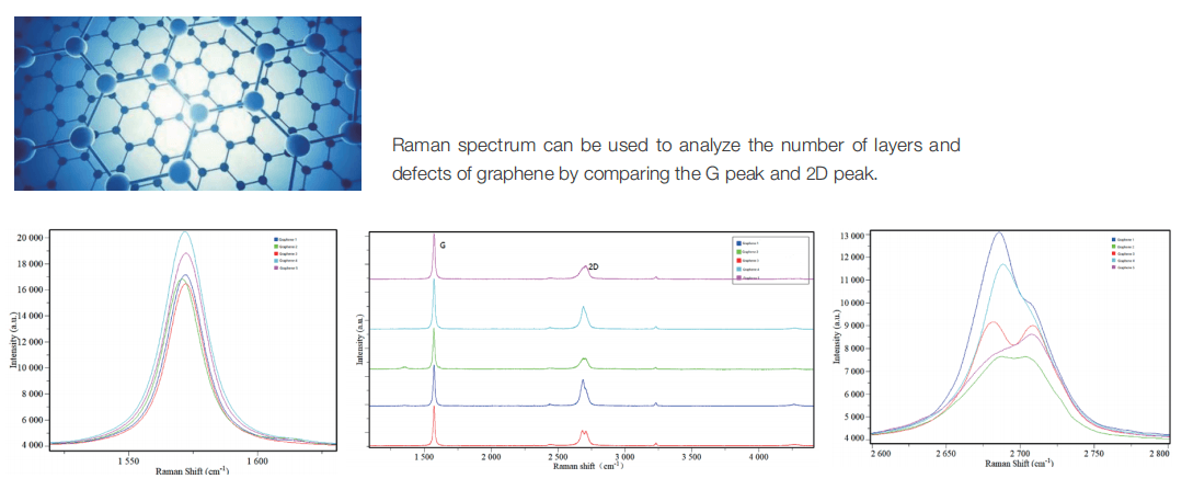
Graphene layer count and defects
Comparing the G and 2D peaks reveals the number of graphene layers and the defect density.
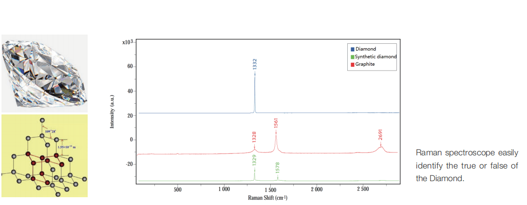
Natural diamond, synthetic diamond and graphite
The 1332 cm⁻¹ diamond line against the 1328 / 1561 / 2691 cm⁻¹ graphite bands separates the three at a glance.
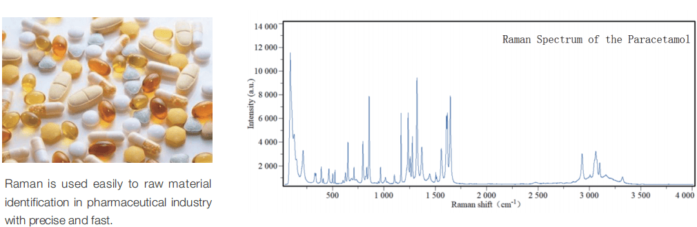
Pharmaceutical raw-material identification
Raman spectrum of paracetamol — fast, precise identification of raw materials in the pharmaceutical industry.
Technical Specifications
System Technical Information
| Parameter | Specification |
|---|---|
| Excitation wavelength | 532 nm, 638 nm or 785 nm (one per system) |
| Laser power | 100 mW (532 nm) · 50 mW (638 nm) · 100 mW (785 nm) |
| Raman shift range | 80–9000 cm⁻¹ @ 532 nm · 80–6000 cm⁻¹ @ 638 nm · 80–3200 cm⁻¹ @ 785 nm |
| Low-wavenumber capability | 80 cm⁻¹ typical, 100 cm⁻¹ guaranteed |
| Spectral resolution | 1.5 cm⁻¹ (532 / 638 nm) · 2.3 cm⁻¹ (785 nm) |
| Signal-to-noise ratio | > 20:1 on the silicon third-order peak |
| Spectrograph | 320 mm focal length, Czerny-Turner |
| Gratings | Three blazed gratings per excitation line (see excitation options) |
| Microscope | Upright only; couples to most upright microscopes |
| Objectives | 10×, 50×, 100× and 50× LWD, semi-apochromatic |
| Epi-illumination | Quartz tungsten halogen, 12 V / 100 W |
| Sample stage | Manual standard; motorised optional for Raman mapping |
Final specifications depend on the selected excitation line, gratings, objectives and stage.
Choosing a Raman System
Where the RTS-mini Sits in the Range
New to the technique? Start with the confocal Raman knowledge base or the Raman measurement design guide.