PIV, confocal, wafer, marking systems
Semiconductor wafer inspectionlaser system
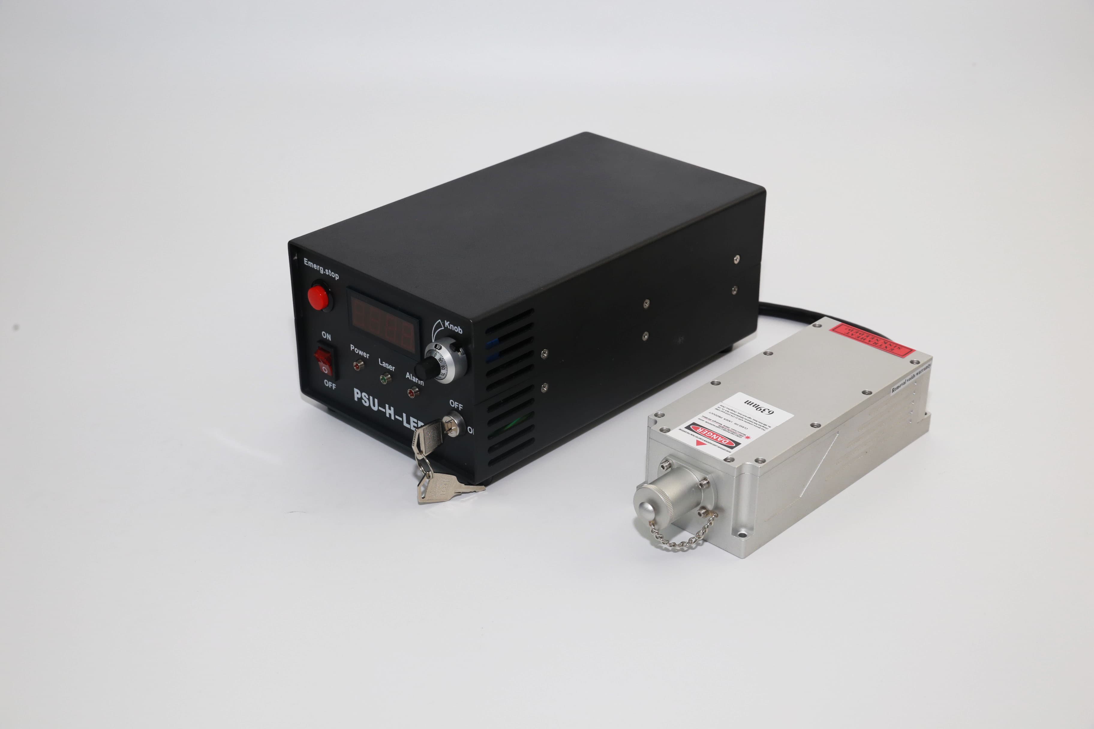
The Semiconductor wafer inspection is a laser source. Output power describes the optical energy delivered per second. At the sample, irradiance also depends on the beam area and losses through the optical path, so the delivered spot must be considered along with the source rating.
Specifications
Semiconductor wafer inspection
1 specification rows
| Beam / notes | Non-destructive or minimally invasive inspection of wafer surface topography, electrical properties, and internal structure, etc. |
|---|
What do you need?
The full datasheet for this model is on request. Tell us the output power, beam quality and beam delivery you need, and we'll reply with the matching configuration and lead time.
Related application systems
Compare the Semiconductor wafer inspection with nearby application systems across the wavelength range.